Method and system for minimizing the accumulated offset error for an analog to digital converter

an analog-to-digital converter and offset error technology, applied in the field of integrated circuits, can solve the problems of offset error in design, offset error in measurement and ideal voltage, offset error in offset compensation, etc., and achieve the effect of high offset error compensation accuracy

Inactive Publication Date: 2009-03-05
ATMEL CORP
View PDF19 Cites 49 Cited by
  • Summary
  • Abstract
  • Description
  • Claims
  • Application Information

AI Technical Summary

Benefits of technology

[0007]A system and method in accordance with the present invention compensates for the accumulated offset error over many samples, thereby achieving much higher accuracy in the offset error compensation. For one implementation in CMOS, the existing methods for automatic offset error cancellation were able to achieve an offset error level of approximately 100 μV, while the method in accordance with the present invention could reduce the accumulated offset error to about 1 μV.

Problems solved by technology

Analog-to-digital converters have a certain offset error.
Offset error is the difference between the measured and ideal voltage at the analog input that produces the midscale code at the outputs.
Even when using such methods, there is some offset error in the design.
Typically, a well-designed differential analog to digital converter implemented in CMOS may have a temperature-dependent offset error of about 100 μV.
In this case, the amount of offset error will accumulate, causing a significant error in the result, particularly if the input levels to the analog digital converter are very low for long periods.
However it is known that this method of offset error cancellation can be inaccurate when the analog to digital converter is utilized over a long period of time because the offset error can accumulate.

Method used


Image

  • Method and system for minimizing the accumulated offset error for an analog to digital converter
  • Method and system for minimizing the accumulated offset error for an analog to digital converter
  • Method and system for minimizing the accumulated offset error for an analog to digital converter

Examples


embodiment 1

[0036]In the first embodiment:

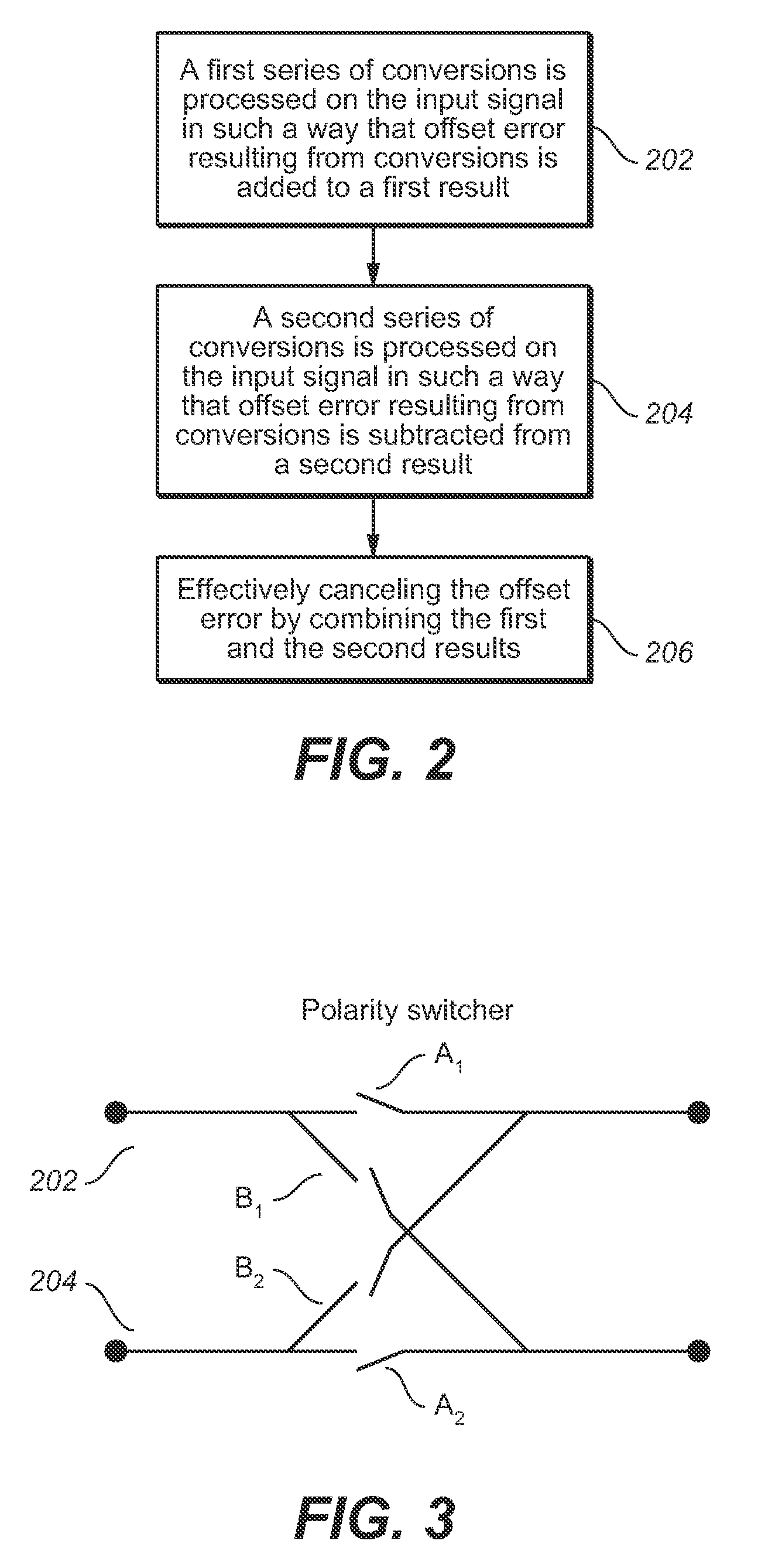
[0037](1) The polarity switcher 110 is added in hardware; and

[0038](2) Software controls the polarity switcher 110 (step 204, FIG. 2).

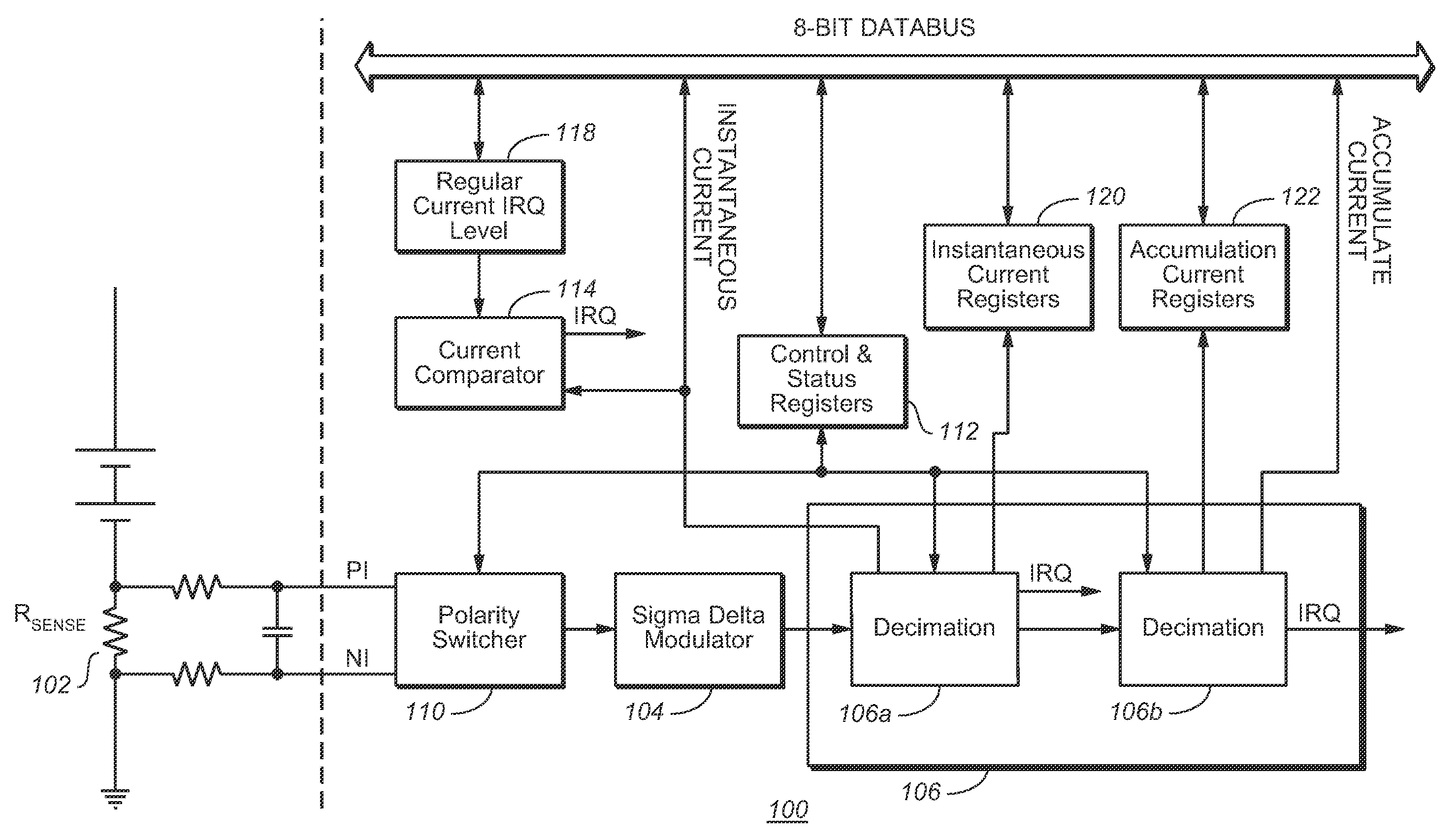
[0039]FIG. 5 is a flow chart which illustrates a software program which provides control of the polarity switch. First, while running the analog to digital conversions, a search is conducted for a time period where the input signal is at a constant input level, via step 402. Thereafter N conversions (I) are run with a positive polarity at the input, followed by N conversions with negative polarity at the input, via step 404. Next it is determined if the input level signal was constant for 2*N conversions, via step 406. Finally, the offset is calculated by the formula offset=(I1+I2+ . . . +I2n) / (2*N) to find the average, via step 408. In so doing, the offset can be measured on a regular basis.

[0040]The flow chart describes an efficient way to measure actual offset without interrupting ongoing ADC conversions. This can be u...

embodiment 2

[0043]In the second embodiment:

[0044](1) The polarity switcher 110 is added in hardware.

[0045](2) Software controls the polarity switcher 110.

[0046]However, in this embodiment, the modulator 104 inverts the output signal before the filter 106. Therefore software no longer needs to invert the results when the polarity switcher 110 is in state 2. This second embodiment also has additional advantages listed below:

[0047]1. The filter 106 is presented a more stable value when the polarity switcher 110 changes.

[0048]2. Any hardware use of the accumulated value needs polarity correction in hardware. Changing polarity at this point gives the lowest cost hardware solution, since the number is typically only 1 bit. One example of hardware use of the accumulated value is the “regular current detection” feature that detects if the value is above a certain limit. This can be performed, for example, by the current comparator 114.

[0049]It is not required to implement the polarity switcher control ...


PUM


Abstract

A method and system utilized with an analog to digital converter is disclosed. The method and system comprise providing a first conversion on an input signal. In the first conversion, an offset error is added to the input signal to provide a first result. The method and system further includes providing a second conversion on the input signal. In the second conversion, an offset error is subtracted from the input signal to provide a second result. The first and second results are then combined to substantially remove the offset error. A system and method in accordance with the present invention compensates for the accumulated offset error over many samples, thereby achieving much higher accuracy in the offset error compensation.

Description

CROSS REFERENCE TO RELATED APPLICATIONS[0001]This application is a continuation-in-part of U.S. patent application Ser. No. 11 / 467,802, filed Dec. 21, 2006, entitled “Current sensing analog to digital converter and method of use”, assigned to the assignee of the present invention and incorporated by reference in its entirety herein and is also related to U.S. Pat. No. 7,113,122, filed Jan. 25, 2005, entitled, “Current sensing analog to digital converter and method of use,” and assigned to the assignee of the present application.FIELD OF THE INVENTION[0002]The present invention relates generally to integrated circuits and more specifically to a current sensing analog to digital converter that is utilized in such circuits.BACKGROUND OF THE INVENTION[0003]Analog-to-digital converters have a certain offset error. Offset error is the difference between the measured and ideal voltage at the analog input that produces the midscale code at the outputs. There are known techniques to minimize...

Claims


Application Information

Patent Timeline
Patent Type & Authority Applications(United States)
IPC IPC(8): H03M1/10H03M1/12
CPCG01R19/0092G01R19/2509H03M3/356H03M1/0656H03M3/34H03M1/0607
Inventor AAS, ARNEGANGSTOE, GUNNARFENHEIM, TORGEIR
Owner ATMEL CORP
Why Eureka
Try Eureka