Imaging apparatus and driving method of ccd type solid-state imaging device

a solid-state imaging and imaging apparatus technology, applied in the field of imaging apparatus, can solve problems such as difficult pixel mixture, and achieve the effect of good pixel addition

Inactive Publication Date: 2009-03-05
FUJIFILM CORP
View PDF4 Cites 6 Cited by
  • Summary
  • Abstract
  • Description
  • Claims
  • Application Information

AI Technical Summary

Benefits of technology

[0012]An object of the invention is to provide, in a CCD type solid-state imaging device having A double arrangement structure of Bayer array, a driving method of the CCD type solid-state imaging device and an imaging apparatus, in which good pixel addition can be performed.

Problems solved by technology

Therefore, the CCD type solid-state imaging device has restriction that detected signals of the respective pixels should be read out in a specific order, so that the pixel mixture is not easy.
However, even in case that pixel addition in the horizontal direction is performed by a CCD type solid-state imaging device having a line memory, when the color filter arrangement of this CCD type solid-state imaging device is the double arrangement structure of Bayer array as described in the lower part in FIG. 6, it is not clear which method of driving the solid-state imaging device should be adopted to perform the pixel addition at an appropriate and high frame rate.

Method used


Image

  • Imaging apparatus and driving method of ccd type solid-state imaging device
  • Imaging apparatus and driving method of ccd type solid-state imaging device
  • Imaging apparatus and driving method of ccd type solid-state imaging device

Examples


Embodiment Construction

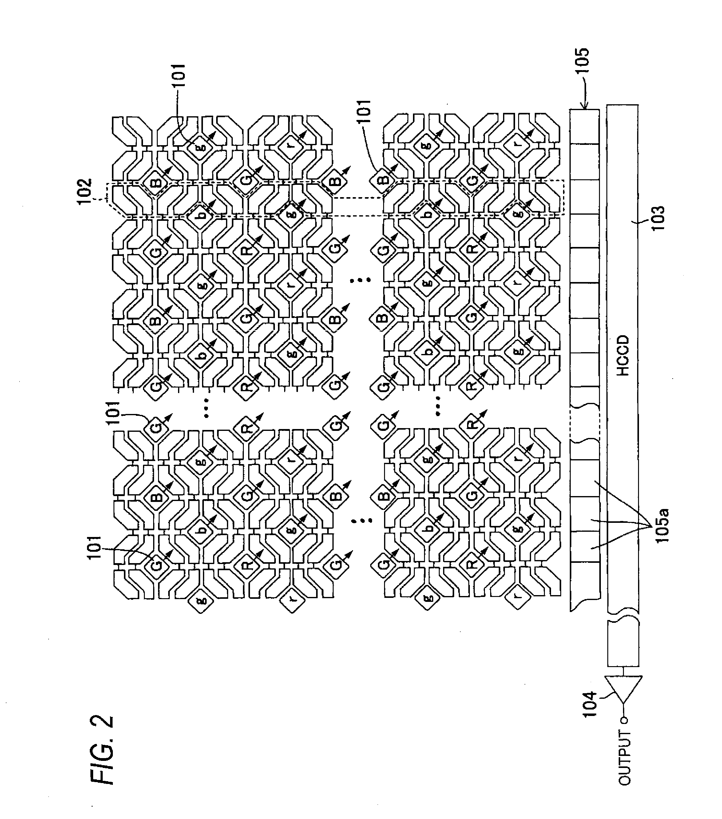
[0026]According to an exemplary embodiment of the invention, pixel addition from a CCD type solid-state imaging device in which the color filter arrangement has a double arrangement structure of Bayer array can be readily and accurately performed at a high frame rate thereby to read out the signals, so that high-sensitivity imaging and moving imaging can become easy.

[0027]An exemplary embodiment of the invention will be described below with reference to drawings.

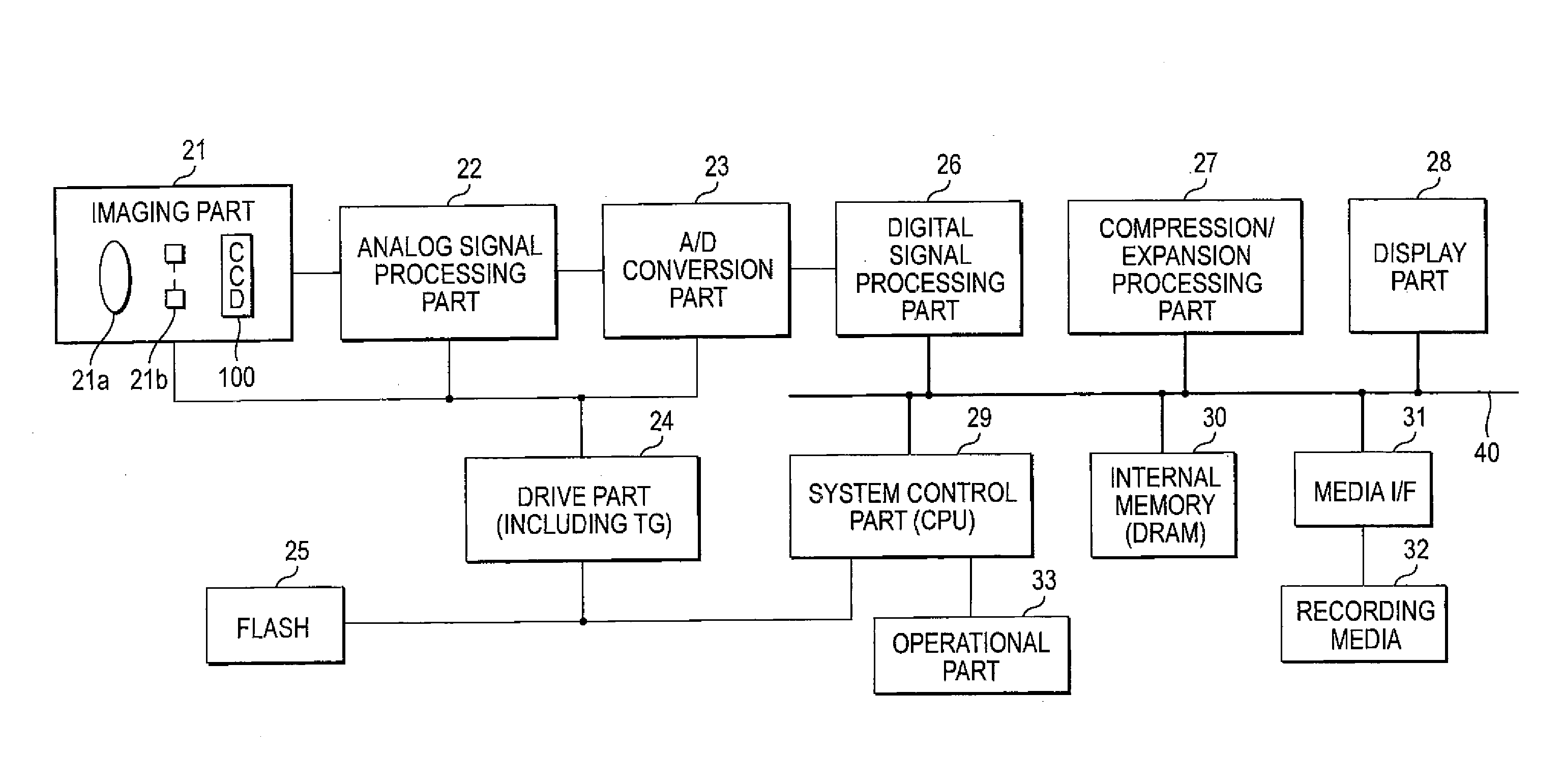
[0028]FIG. 1 is a functional block diagram of a digital camera according to an exemplary embodiment of the invention. This digital camera includes an imaging part 21; an analog signal processing part 22 which subjects analog image data outputted from the imaging part 21 to analog processing such as automatic gain control (AGC) and correlated double sampling (CDS); an analog / digital conversion part (A / D) 23 which converts analog image data outputted from analog signal processing part 22 into digital image data; a drive part (...


PUM


Abstract

There is provided a driving method of a CCD solid-state imaging device that includes: a first pixel group including pixels arranged in a square lattice; a second pixel group including pixels shifted in a row direction and a column direction of the square lattice by 2 / 1 of a pixel pitch with respect to the pixels in the first pixel group; color filters arranged in Bayer array with respect to each of the first pixel group and the second pixel group; vertical transfer paths; a horizontal charge transfer path; and a line memory. The method includes adding signal charges, which are detected in two same color pixels adjacent in a horizontal direction in the first pixel group, in the horizontal charge transfer path and outputting the added signal charges, by means of a four-phase drive pulse of the horizontal charge transfer path and a drive pulse of the line memory.

Description

[0001]This application is based on and claims priority under 35 U.S.C. §119 from Japanese Patent Application No. 2007-219893 filed Aug. 27, 2007, the entire disclosure of which is herein incorporated by reference.BACKGROUND OF THE INVENTION[0002]1. Field of the Invention[0003]The present invention relates to an imaging apparatus including a CCD (Charge Coupled Device) type solid-state imaging device, and particularly to a driving method of the CCD type solid-state imaging device.[0004]2. Description of Related Art[0005]As an array pattern of color filters stacked on respective pixels of a solid-state imaging device, there is a Bayer array. This Bayer array is constituted, as shown on an upper part in FIG. 6, so that: when three-primary-color type color filters of red (R, r), green (G, g), and blue (B, b) are arranged on pixels (photoelectric conversion element: photodiode) formed in a square lattice shape in a surface part of a semiconductor substrate, a row in which each red filter...

Claims


Application Information

Patent Timeline
Patent Type & Authority Applications(United States)
IPC IPC(8): H04N5/335H01L27/148H04N5/341H04N5/347H04N5/349H04N5/351H04N5/369H04N5/372H04N5/376
CPCH04N5/3458H04N9/045H04N5/347H04N25/46H04N25/447H04N25/134
Inventor SAKAMOTO, TOMOHIRO
Owner FUJIFILM CORP
Why Eureka
Try Eureka