Suction apparatus, polishing apparatus, semiconductor device, and method of manufacturing a semiconductor device

a technology of polishing apparatus and suction apparatus, which is applied in the direction of grinding drives, manufacturing tools, lapping machines, etc., can solve the problems of inability to completely remove foreign materials, inability to completely eliminate foreign materials, and the possibility of foreign materials interposing therebetween, so as to reduce the effect of caused, prevent localized excessive polishing, and increase the material planarization

Active Publication Date: 2009-03-05
NIKON CORP
View PDF17 Cites 27 Cited by
  • Summary
  • Abstract
  • Description
  • Claims
  • Application Information

AI Technical Summary

Benefits of technology

[0027]According to the present invention described above, a suction apparatus able to reduce the effect caused by foreign materials and, moreover, able to increase the planarization of the material to be suctioned in the suctioned state can be provided.
[0028]In addition, according to the present invention, a polishing apparatus

Problems solved by technology

When a foreign material becomes interposed between the wafer and the suction surface of the suction apparatus, the wafer deforms and forms a bulge in proximity of the location of the foreign material that, in turn, results in various undesirable outcomes.
For example, when polishing is performed to planarize the wafer, excessive polishing will occur in the location in which the bulge has been produced by the foreign material and will result in a fatal defect thereof.
Although the wafer and the suction surface of the suction apparatus are normally washed, it is impossible to completely remove such foreign materials.
Although the contact surface area between the wafer and the suction surface of the aforementioned conventional suction apparatuses disclosed in Japanese Unexamined Patent Application Publication Nos. 2002-217141 and H10-50810 can be regarded as small, the possibility that a foreign material will become interposed therebetween cannot be completely eliminated.
When a foreign material becomes interposed between the wafer and the tip-end faces of the protrusions in the aforementioned conventional suction apparatuses, as described above, the wafer deforms and forms a bulge in proximity of the location of the foreign material which, in turn, results in various undesirable outcomes.
However, in the aforementioned conventional art proposed in Japanese Unex

Method used


Image

  • Suction apparatus, polishing apparatus, semiconductor device, and method of manufacturing a semiconductor device
  • Suction apparatus, polishing apparatus, semiconductor device, and method of manufacturing a semiconductor device
  • Suction apparatus, polishing apparatus, semiconductor device, and method of manufacturing a semiconductor device

Examples


first example

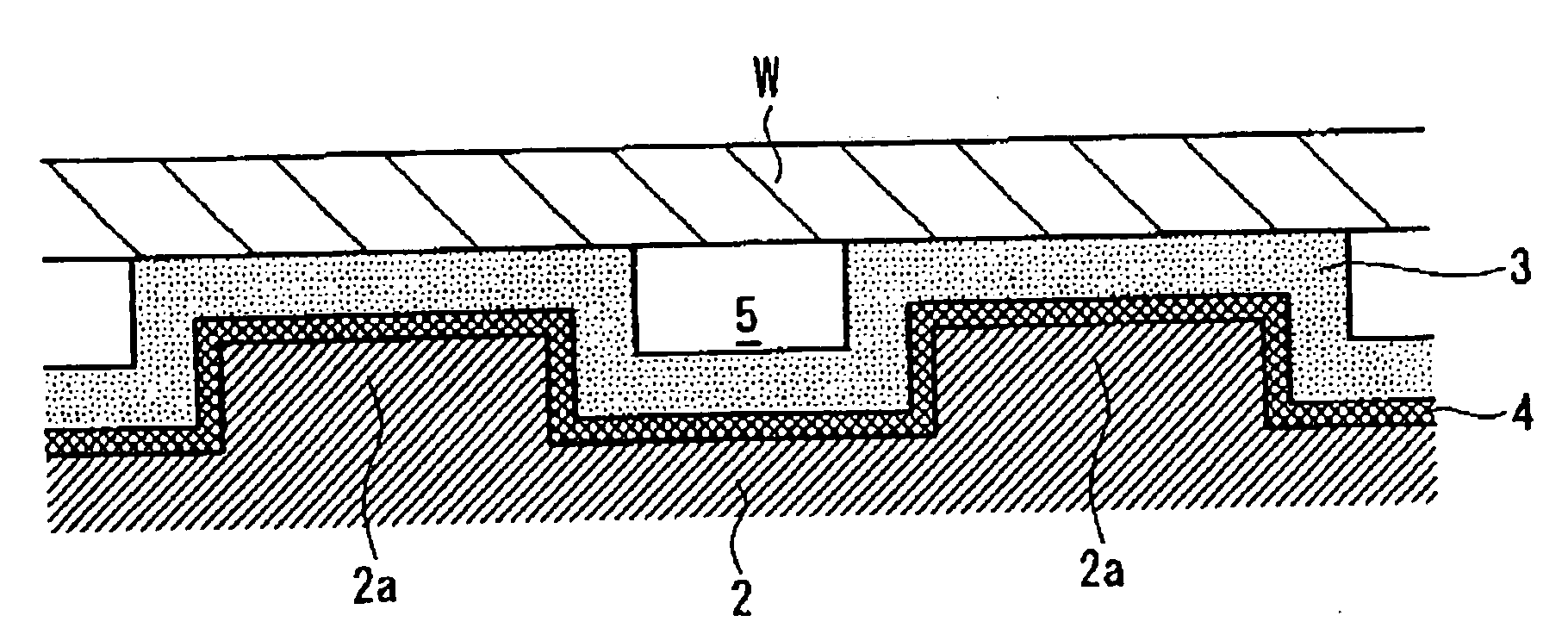
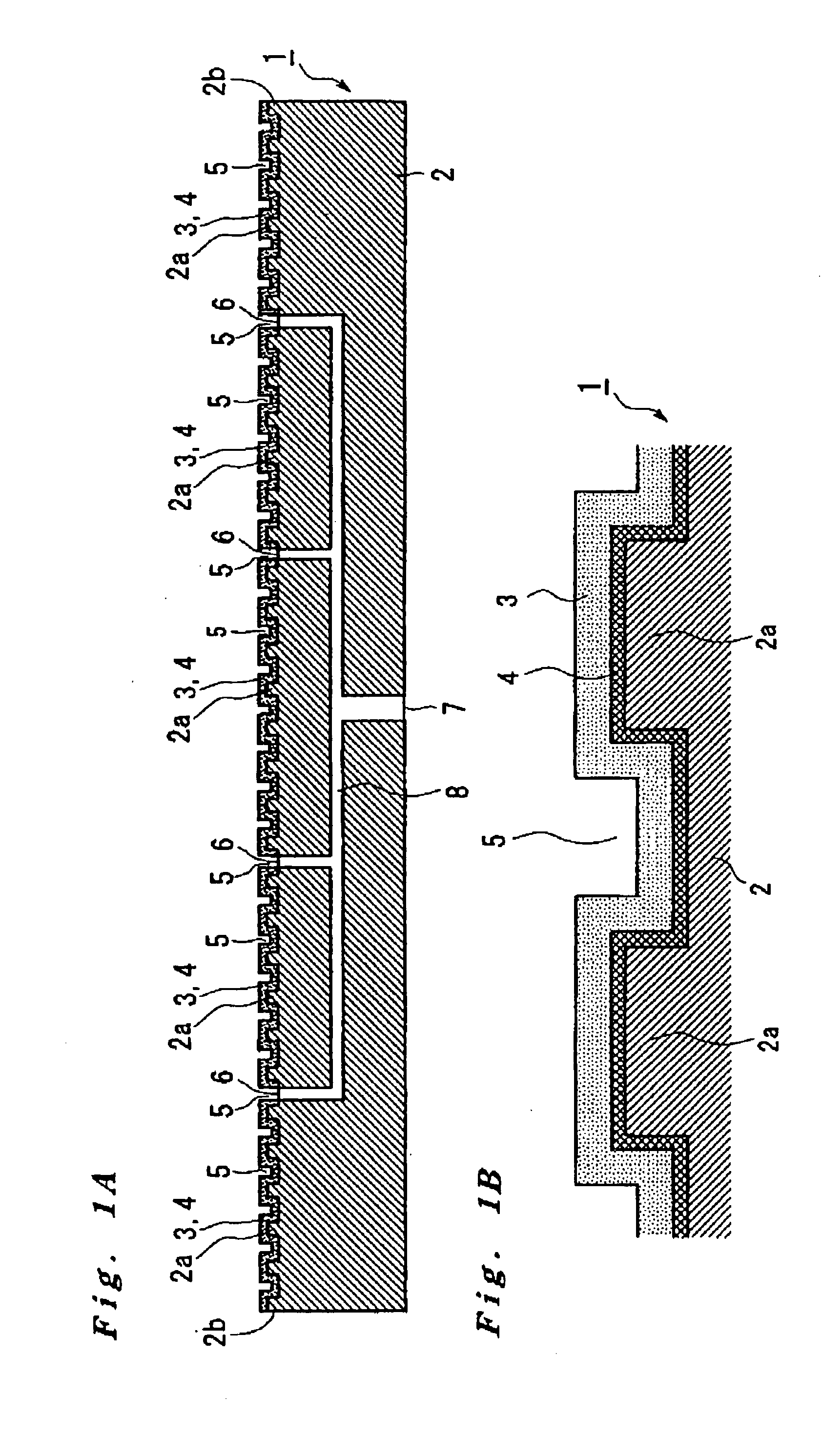
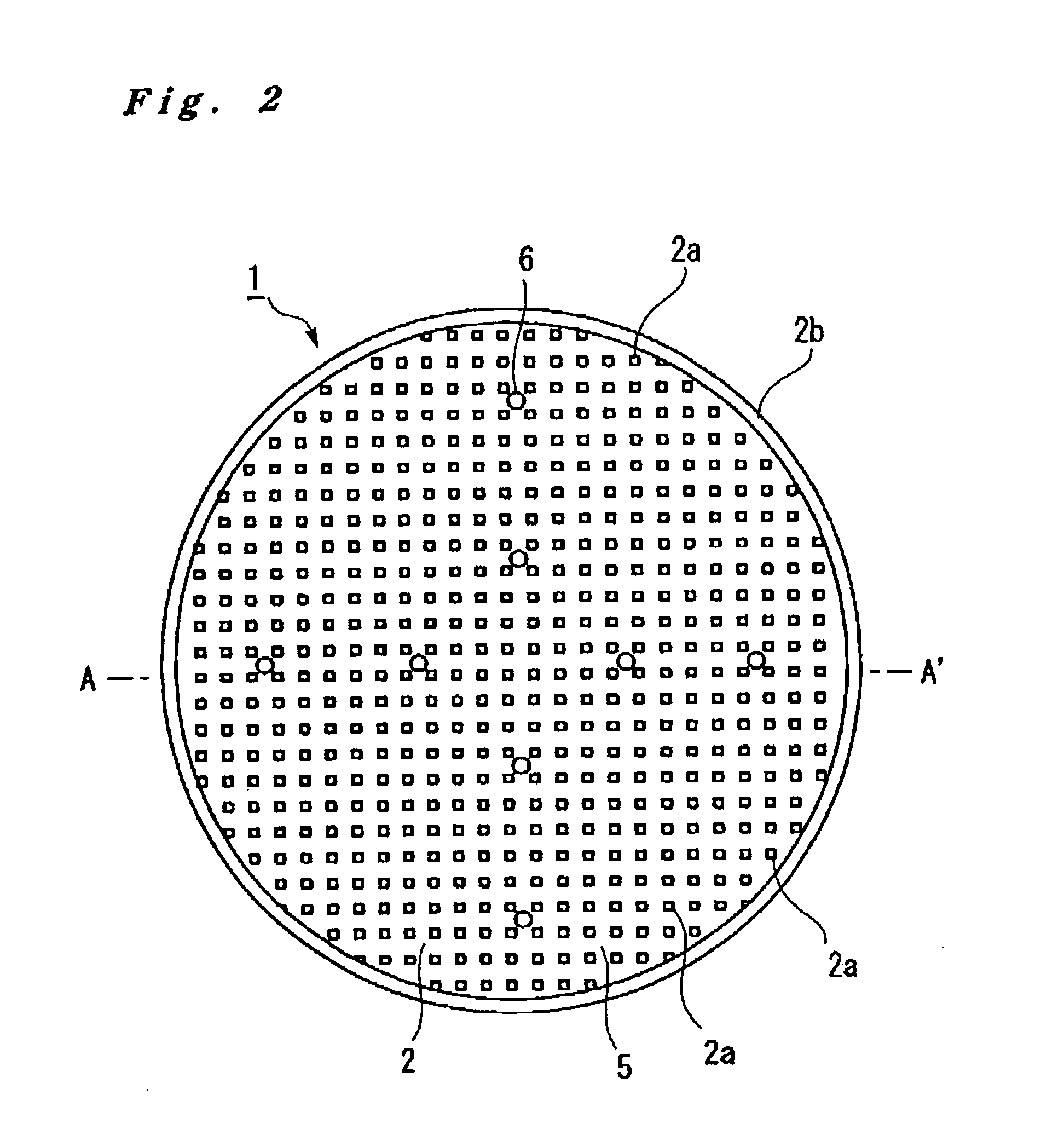
[0038]FIG. 1(a) is a schematic cross-sectional view of a suction apparatus 1 of a first embodiment of the present invention. FIG. 1(b) is a partially expanded schematic cross-sectional view of FIG. 1(a). FIG. 2 is a schematic cross-sectional view of the suction apparatus 1 of FIG. 1. A coating layer 3 and undercoat layer 4 have been omitted from the illustration of FIG. 2.

[0039]The suction apparatus 1 of this embodiment is configured to suction-hold a wafer W serving as a material to be suctioned, that is to say, it is configured as a wafer chuck.

[0040]As shown in FIG. 1 and FIG. 2, this suction apparatus 1 comprises a disk-like suction substrate 2, a coating layer 3, and an undercoat layer 4.

[0041]The suction substrate 2 is configured from, for example, a ceramic such as alumina or stainless steel and is rigid. A large number of pin-like protrusions 2a are formed in an upper-surface side (side to which the material to be suctioned is suctioned) of the suction substrate 2. These pro...

second example

[0069]FIG. 5 is a schematic cross-sectional view of a suction apparatus 21 of a second embodiment of the present invention correspondent to FIG. 2. Elements of FIG. 5 identical to the elements of FIG. 1 and FIG. 2 are denoted using identical symbols and a repetition of the description thereof has been omitted. In FIG. 5, similarly to FIG. 2, the illustration of the coating layer 3 and undercoat layer 4 has been omitted.

[0070]The suction apparatus 21 of this embodiment differs from the suction apparatus 1 of the first embodiment described above in that a plurality of ring-like ridges protrusions 2c are formed in the upper surface of the suction substrate 2 instead of pin-like protrusions 2a, and in that the number and arrangement of the through-holes 6 has been altered in accordance therewith. The plurality of protrusions 2c are arranged concentrically with the ring-like ridge protrusion 2b arranged in the outer perimeter part. While not shown in the diagram, the coating layer 3 of t...

third example

[0073]FIG. 6 is a schematic cross-sectional view that schematically shows a polishing apparatus of a third embodiment of the present invention.

[0074]The polishing apparatus of this embodiment comprises a polishing tool 51, a wafer chuck 52 for holding a wafer serving as the material to be suctioned on the lower side of the polishing tool 51, and a polishing agent supply unit (not shown in the diagram) for supplying a polishing agent (slurry) between the wafer W and polishing tool 51 by way of a supply path formed in the polishing tool 51 (not shown in the diagram).

[0075]Using a mechanism not shown in the diagram employing an electric motor or the like as an actuator, the polishing tool 51 can be rotated and oscillated (reciprocally moved) up and down and left to right as shown by the arrows a, b, c of FIG. 6. The wafer chuck 52 can be rotated as shown by the arrow t shown in FIG. 6 by a rotating table 53 not shown in the diagram employing a power motor or the like as an actuator. Wh...


PUM


Abstract

A suction apparatus 1 holds a wafer W by performing vacuum-suctioning on the wafer W. The suction apparatus 1 comprises a suction substrate 2. The suction substrate 2, which is rigid, comprises a plurality of pin-like protrusions 2a formed so that the tip-end faces (upper surfaces) thereof are the same height. An elastic coating layer is coated by way of an undercoat layer 4 on the tip-end faces of the protrusions 2a. When the wafer W is suctioned, even if a foreign matter is interposed between the wafer W and the suction surface, because the foreign matter embeds itself into the coating layer 3, the planarization of the wafer W is improved. In addition, because the coating layer 3 can be made comparatively thinner, undulations in the wafer W can be reduced and, to that end, the planarization of the wafer W in the suctioned state can be improved.

Description

FIELD OF THE INVENTION[0001]The present invention relates to a suction apparatus for holding a material to be suctioned such as a wafer or other substrate by vacuum-suctioning the material to be suctioned, a polishing apparatus that employs this suction apparatus, and a semiconductor device and method of manufacturing a semiconductor device.BACKGROUND OF THE INVENTION[0002]In conventionally known suction apparatuses for holding a material to be suctioned such as a wafer or other substrate by vacuum-suctioning the material to be suctioned, a rigid suction substrate comprising a plurality of pin-like or ridged protrusions of which the tip-end faces thereof are the same height is formed on the side of the suction apparatus to which the material to be suctioned is suctioned (for example, Japanese Unexamined Patent Application Publication Nos. 2002-217141 and H10-50810).[0003]In these suction apparatuses, a negative pressure is created in depressions between the protrusions in a state in...

Claims


Application Information

Patent Timeline
IPC IPC(8): H01L21/67B24B37/30B24B41/06H01L21/304H01L21/683
CPCB24B37/30B24B41/061B23Q3/088H01L21/6875H01L21/6838B23Q3/08H01L21/683H01L21/304B24B37/04
Inventor ASADA, NAOKI
Owner NIKON CORP
Why Eureka
Try Eureka