Solid imaging device

Inactive Publication Date: 2009-03-12
RENESAS ELECTRONICS CORP
View PDF3 Cites 1 Cited by
  • Summary
  • Abstract
  • Description
  • Claims
  • Application Information

AI Technical Summary

Benefits of technology

[0020]According to the present invention, electric charges can be outputted at the same data rate at any resolutions, thus facilitating sampling. In particular, effects can be exhibited in a system using a plurality of chips such as CIS.

Problems solved by technology

High-frequency noise is generated more easily which causes EMI (electro magnet interference).
The same problem is caused in FIG. 5 when the resolution is gradually decreased.
If the problem is intentional to be eliminated by increasing the number of photodiodes, an output order of data in each of resolutions becomes complicated, thereby raising another problem of the increase in the number of read gates.
In other words, a same clock signal is supplied to both of the first and second electric charge transfer sections, and therefore, they cannot be driven at different timings or in different cycles.

Method used


Image

  • Solid imaging device
  • Solid imaging device
  • Solid imaging device

Examples


first embodiment

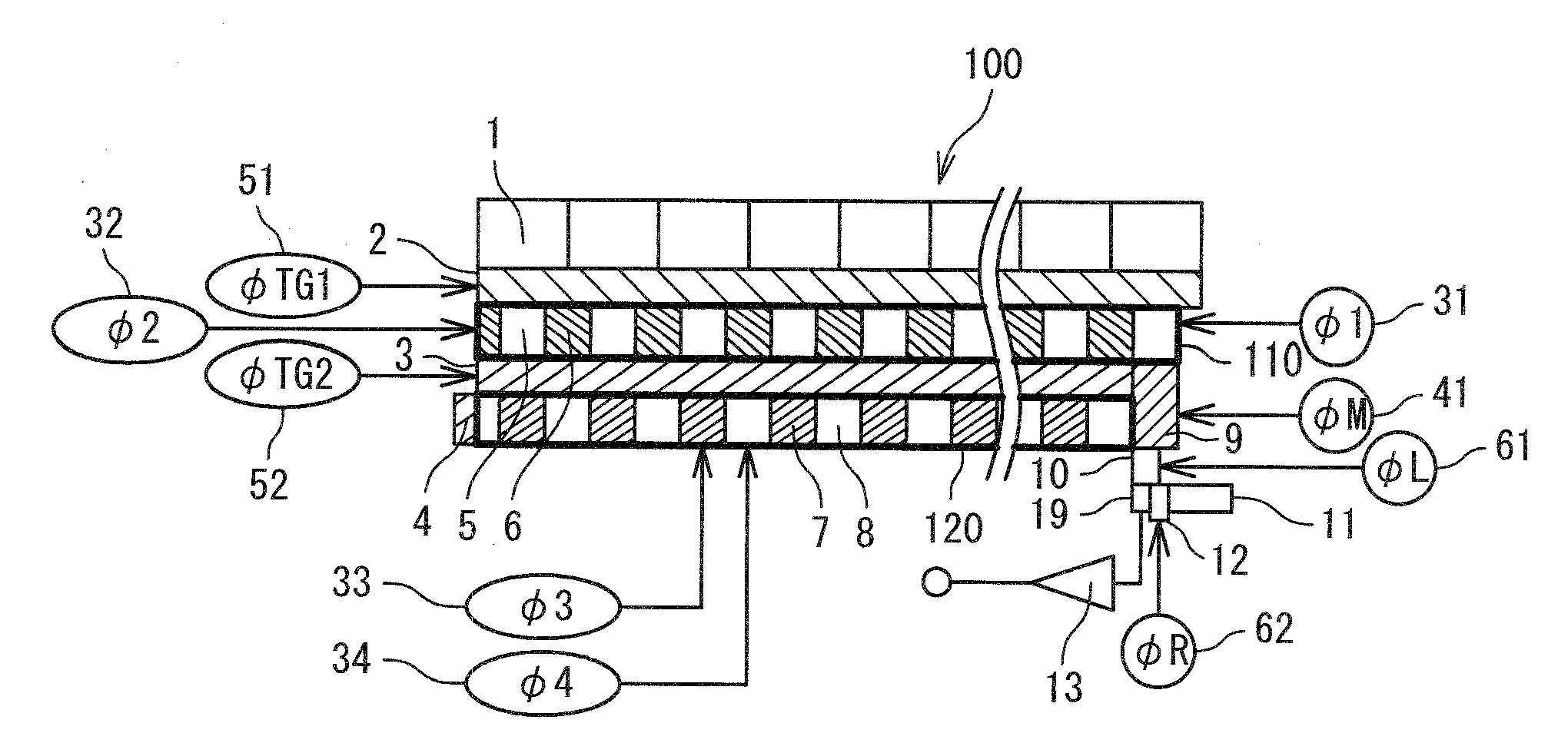
[0055]Referring to FIG. 10, a solid imaging device 100 according to a first embodiment of the present invention will be described. The solid imaging device 100 in the first embodiment includes photodiodes 1 in a photoelectric converting section, a read gate electrode 2, a read gate electrode 3, an overflow drain section 4, transfer electrodes 5, transfer electrodes 6, transfer electrodes 7, transfer electrodes 8, an electric charge coupling electrode 9, a last gate electrode 10, a reset drain 11, a reset gate 12, an amplifier 13 and a floating diffusion capacitance section 19.

[0056]The photodiodes 1 perform photoelectric conversion to convert light into an electric charge. The read gate electrode 2 sends the electric charges obtained through photoelectric conversion to the transfer electrodes 5. Then, the electric charges are sent to the transfer electrode 8 as will be described later. The read gate electrode 3 sends the electric charges accumulated in the transfer electrodes 8 to t...

second embodiment

[0069]The solid imaging device according to a second embodiment of the present invention will be described in detail with reference to the attached drawings. The transfer time from the first electric charge transfer section 110 to the second electric charge transfer section 120 in the first embodiment has larger effects on an output time as the resolution becomes lower. If the effects are unallowable, it is construed to increase the number of chips or increase the frequency only when electric charges are transferred from the first electric charge transfer section 110 to the second electric charge transfer section 120. A structural improvement in the second embodiment is illustrated in FIG. 17.

[0070]As illustrated in FIG. 17, the solid imaging device 100 according to the present invention includes the photodiodes 1 in the photoelectric converting section, the read gate electrode 2, the overflow drain section 4, the transfer electrodes 5, the transfer electrodes 6, the transfer electr...

third embodiment

[0087]Next, the solid imaging device according to a third embodiment of the present invention will be described below.

[0088]When the read period of the electric charges is elongated or a temperature becomes high, a dark current increases in the electric charge transfer section to possibly cause noise.

[0089]First of all, a description will be given on a dark current in the electric charge transfer section in case of no overflow drain section 4 in order to describe functions of the overflow drain section 4 in the first and second embodiments.

[0090]FIG. 26 is timing charts, and FIGS. 27A to 27E shows states of charges.

[0091]FIG. 27A corresponds to a period t0 in FIG. 26. Here, the transfer clock signals which are not currently used are stopped entirely so as to reduce current consumption. Therefore, in addition to electric charges 23 accumulated in the photodiodes 1 in the photoelectric converting section, electric charges corresponding to dark current 28 are accumulated in the first e...


PUM


Abstract

In a solid imaging device, a photoelectric converting section is configured to generate electric charges through photoelectric conversion, and a first charge transfer section is connected with the photoelectric converting section. A first read gate section is provided between the photoelectric converting section and the first charge transfer section, and is configured to transfer the electric charges from the photoelectric converting section to the first charge transfer section. A second charge transfer section operates independently from the first charge transfer section and configured to receive the electric charges transferred from the first charge transfer section.

Description

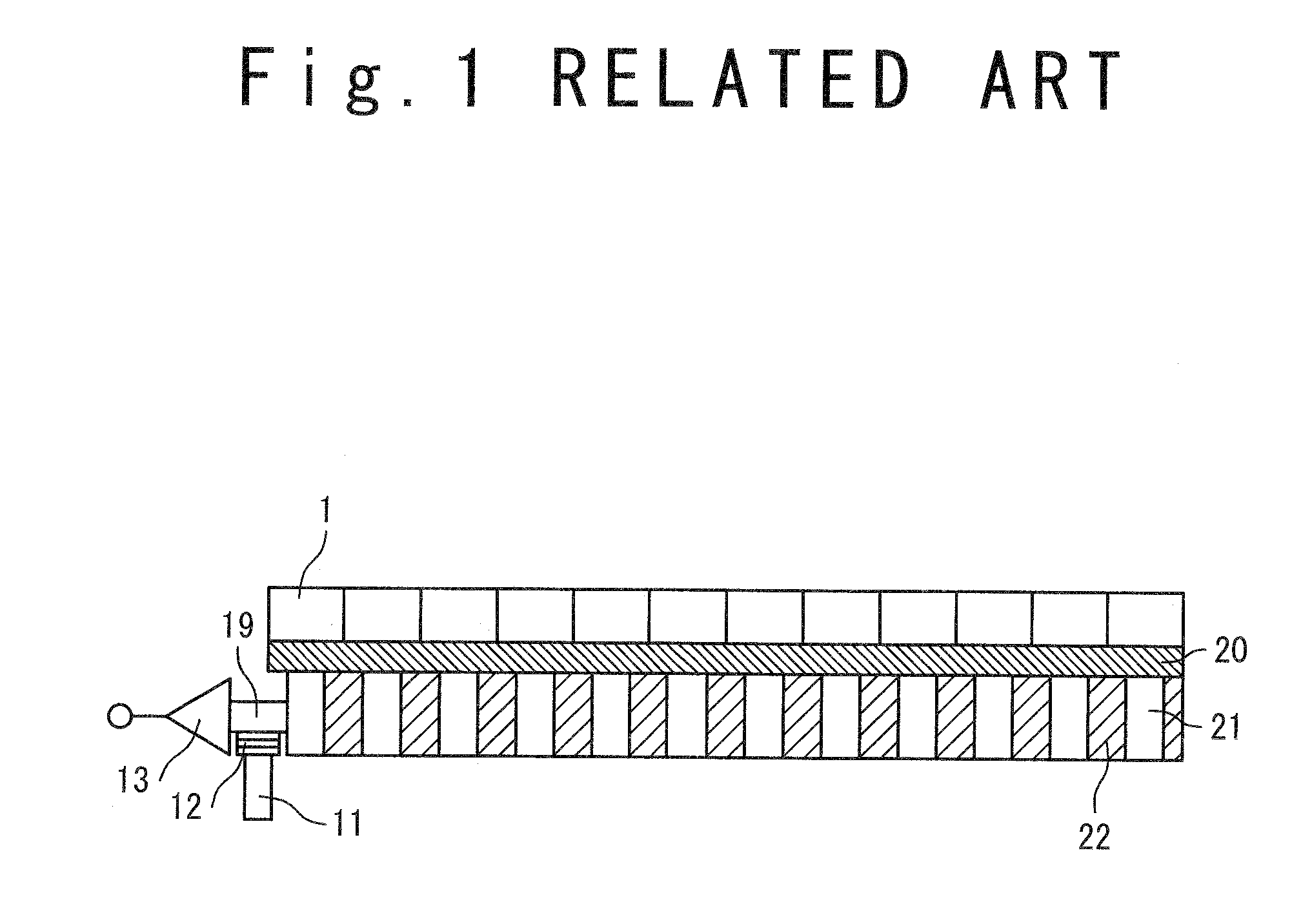
INCORPORATION BY REFERENCE[0001]This application claims priorities on convention based on Japanese Patent Application Nos. 2007-231921 and 2008-179597. The disclosures thereof are incorporated herein by reference.BACKGROUND OF THE INVENTION[0002]1. Field of the Invention[0003]The present invention relates to a solid imaging device and a driving method for the same.[0004]2. Description of Related Art[0005]A solid imaging device used to pick up an image in a scanner has pixels for a number corresponding to a maximum resolution. The resolution is reduced by combining adjacent pixels to a low resolution, thereby shortening an accumulation time.[0006]FIG. 1 is a diagram illustrating a first example of a conventional solid imaging device. This solid imaging device includes photodiodes (i.e., photoelectric converting section) 1 for performing photoelectric conversion, a read gate electrode 20 for sending electric charges (CHG) obtained through the photoelectric conversion to a transfer ele...

Claims


Application Information

Patent Timeline
IPC IPC(8): H04N5/335H01L27/148H04N5/345
CPCH01L27/14609H01L27/14643H04N5/3728H01L27/14887H04N5/335H01L27/14843H04N25/00H04N25/73
InventorFUTAMURA, FUMIAKIKIMURA, TETSUJI
OwnerRENESAS ELECTRONICS CORP