Semiconductor memory device

Inactive Publication Date: 2009-03-19
ELPIDA MEMORY INC
View PDF3 Cites 24 Cited by
  • Summary
  • Abstract
  • Description
  • Claims
  • Application Information

AI Technical Summary

Benefits of technology

[0045]According to the present invention, it is possible to provide a highly integrated

Problems solved by technology

Recently, it has become difficult to miniaturize transistors any further as the demand for high integration grows.
Consequently, it becomes difficult to control a threshold voltage.
However, the means has the problem of increasing the junction leakage of a cell transistor in a DRAM, thus degrading the refresh characteristics of the DRAM.
However, as a problem when the vertical transistor is used as a cell transistor, there is mentioned an increase in word-line resistance.
Furthermore, it is difficult to form a laminated struct

Method used


Image

  • Semiconductor memory device
  • Semiconductor memory device
  • Semiconductor memory device

Examples


Embodiment Construction

[0086]The invention will be now described herein with reference to illustrative embodiments. Those skilled in the art will recognize that many alternative embodiments can be accomplished using the teachings of the present invention and that the invention is not limited to the embodiments illustrated for explanatory purposes.

[0087]Referring to FIG. 1, a semiconductor device according to a first embodiment of the present invention applied to a DRAM will be described.

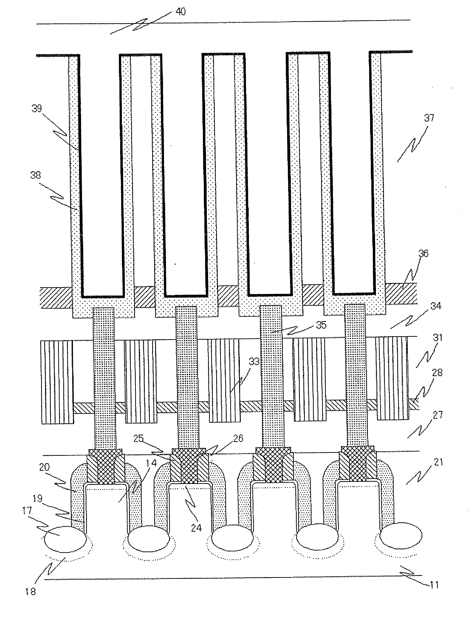
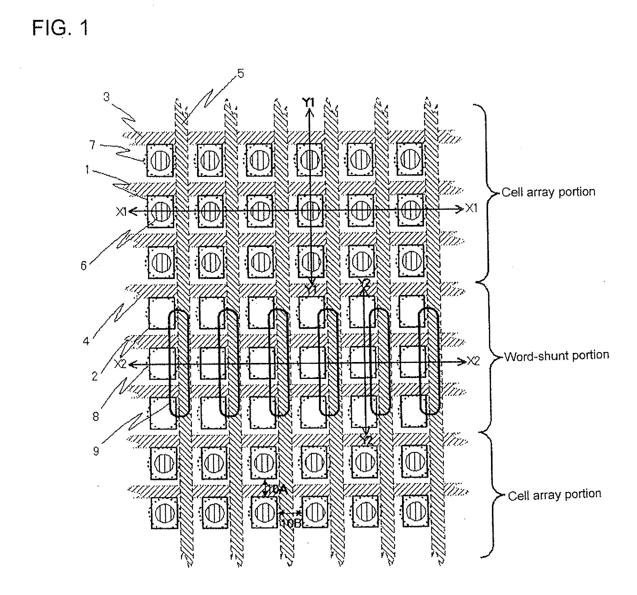
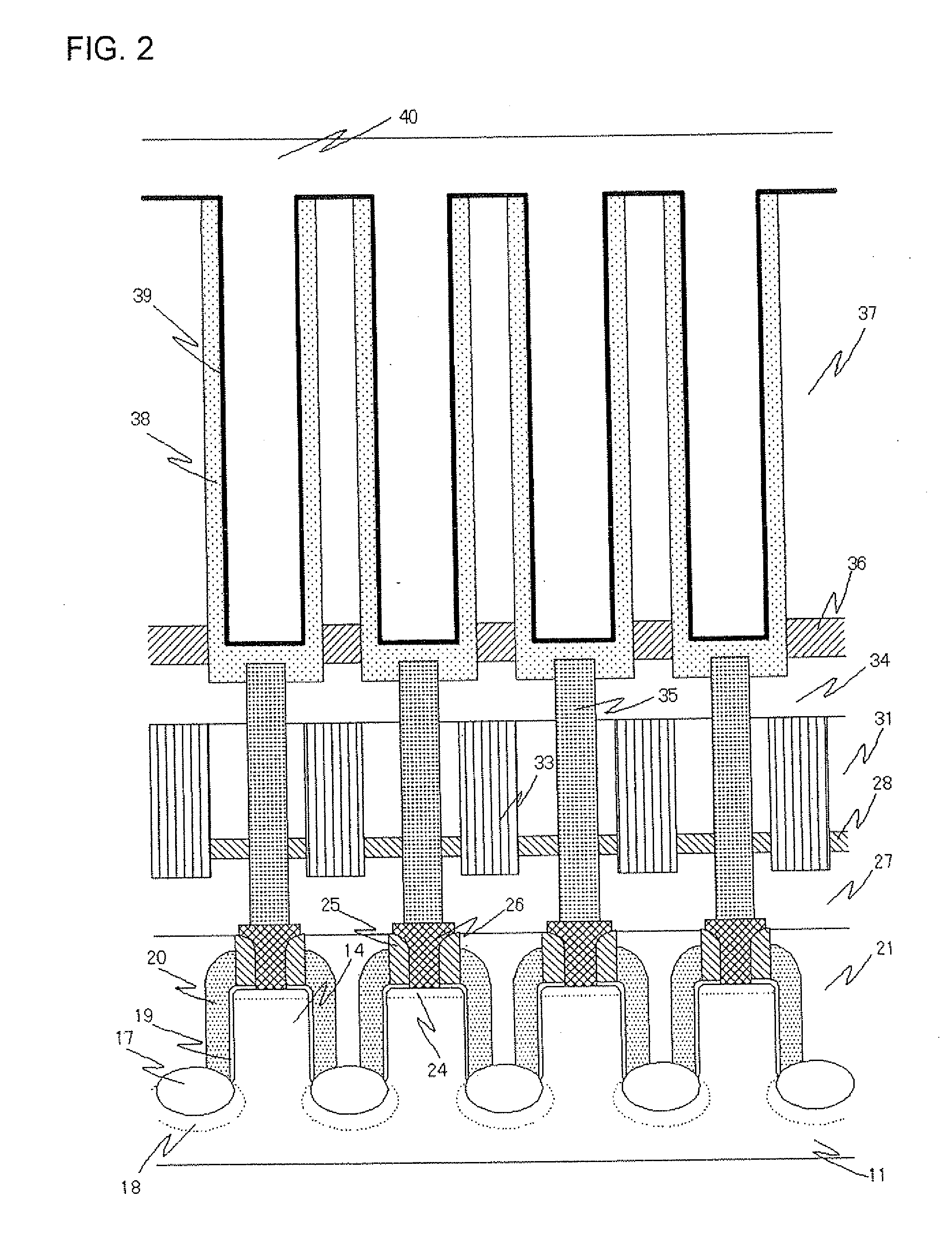
[0088]FIG. 1 illustrates the layout (4F2 cell layout) of a memory cell of the present exemplary embodiment; FIG. 2 illustrates the cross-section structure of a cell array portion as viewed along the line X1-X1 of FIG. 1; FIG. 3 illustrates the cross-section structure of a word-shunt portion as viewed along the line X2-X2 of FIG. 1; FIG. 4 illustrates the cross-section structure of a cell array portion as viewed along the line Y1-Y1 of FIG. 1; and FIG. 5 illustrates the cross-section structure of a word-shunt portion as vie...


PUM


Abstract

A semiconductor memory device includes: first word lines; second word lines, each of the second word lines being electrically connected to a corresponding one of the first word lines; bit lines; and memory cells, each of the memory cells including a transistor and a capacitor. The semiconductor memory device includes: a first cell array portion in which the memory cells are arrayed; and a second cell array portion in which dummy cells, the first word lines and the bit lines are located in the same layout as the first cell array portion. In the second cell array portion, conductive plugs are provided, each of the conductive plugs connecting one of the first word lines and a corresponding one of the second word lines.

Description

BACKGROUND OF THE INVENTION[0001]1. Field of the Invention[0002]The present invention relates to a semiconductor memory device.[0003]2. Description of Related Art[0004]Conventionally, a transistor-miniaturizing technique has been used mainly in order to cope with the high integration of a semiconductor memory device. Recently, it has become difficult to miniaturize transistors any further as the demand for high integration grows. For example, if the gate length L of a cell transistor in a DRAM (Dynamic Random Access Memory) becomes extremely short, the short channel effect of the cell transistor becomes increasingly significant. Consequently, it becomes difficult to control a threshold voltage. In addition, the S value of the cell transistor increases and, from the viewpoint of reduction in the off-state current of the transistor, there arises the need for an even higher threshold voltage.[0005]Means for shallowing the source and drain diffusion layers of a transistor is available a...

Claims


Application Information

Patent Timeline
IPC IPC(8): H01L27/108
CPCH01L27/0207H01L27/10897H01L27/10891H01L27/10876H10B12/50H10B12/053H10B12/488
Inventor TAKAISHI, YOSHIHIRO
Owner ELPIDA MEMORY INC
Why Eureka
Try Eureka