Edge termination for high voltage semiconductor device

a technology of high-voltage semiconductors and edge terminations, which is applied in the direction of semiconductor devices, semiconductor/solid-state device details, electrical apparatus, etc., can solve the problems of depletion and inversion of light-doped p-type surfaces, degrading their ability to sustain voltage, etc., and achieves the effect of high-voltage termination structures

Inactive Publication Date: 2009-03-19
MICROSEMI CORP ANALOG MIXED SIGNAL GRP LTD
View PDF8 Cites 17 Cited by
  • Summary
  • Abstract
  • Description
  • Claims
  • Application Information

AI Technical Summary

Benefits of technology

[0011]An improved high voltage p-channel semiconductor device comprising a p-channel metal oxide semiconductor field effect channel region in a central active area and a high voltage termination structure at the periphery of the device is disclosed.

Problems solved by technology

Due to the field effect, lightly doped p-type surfaces are particularly prone to depletion and inversion from positive charges abundantly present in dielectric films placed in contact with the surface to protect it from scratches or other mechanical damage.
Regardless of the source of these positive charges, the field effect alters the effective spacing of the termination structure and degrades its ability to sustain voltage.

Method used


Image

  • Edge termination for high voltage semiconductor device
  • Edge termination for high voltage semiconductor device
  • Edge termination for high voltage semiconductor device

Examples


first embodiment

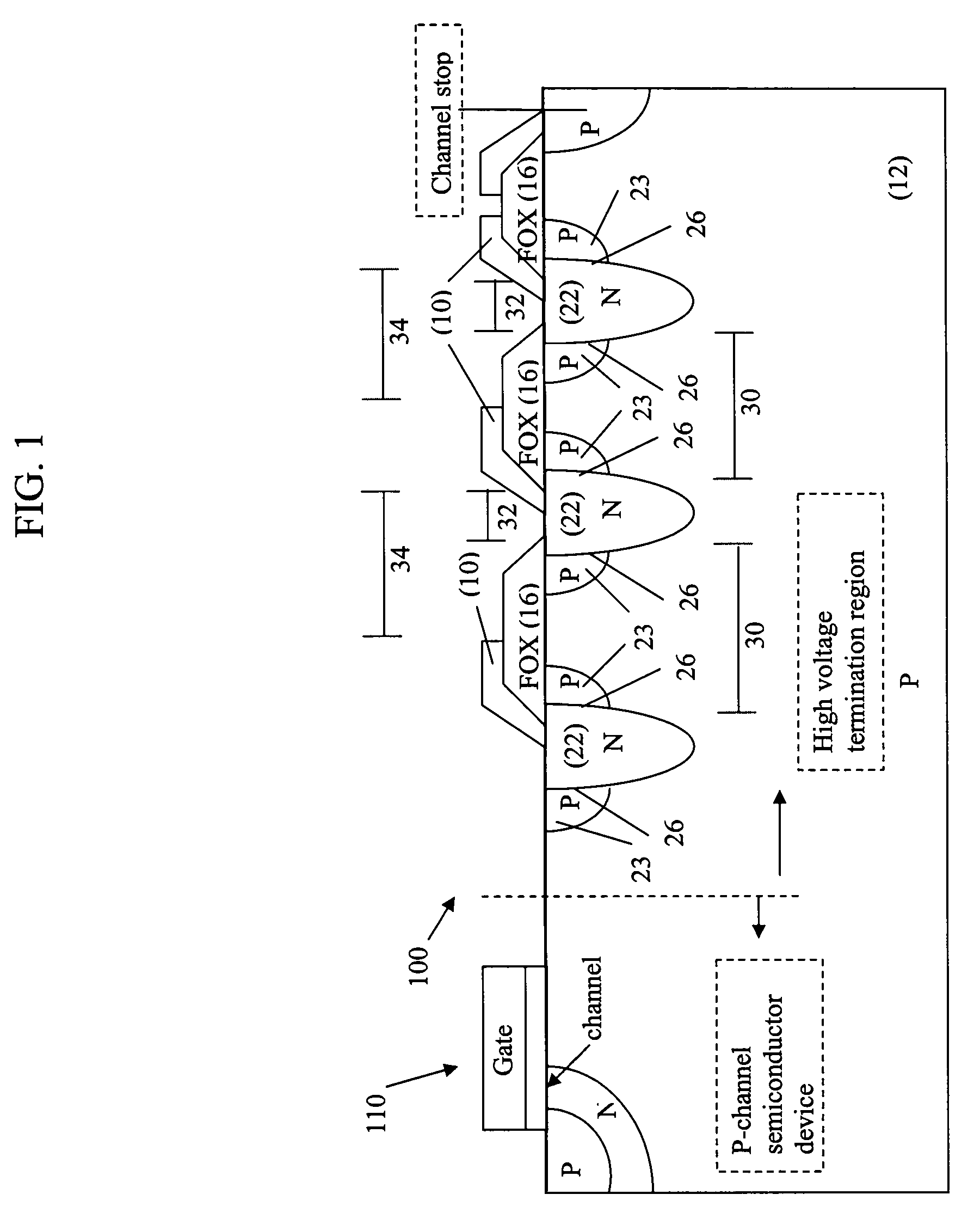
[0026]FIG. 1 is a cross-sectional view of a high-voltage termination structure (100) surrounding a central active device area (110) and having second termination regions on each side of a first termination region according to the present invention.

[0027]Referring to FIG. 1, a high voltage termination structure (100) is a ring-like structure which comprises a p-type substrate (12), n-type first termination regions (22), p-type second termination regions (23), field oxide rings (16) on the substrate surface spanning the gaps (30) between regions (23), and representative field plates (10), capacitively or resistively coupled to the first termination regions (22). At the extreme edge, the termination structure (100) has a field plate (10) and a channel stop region. In this first embodiment, p-type second termination regions are placed on both edges of the first termination regions adjoining and forming a PN junction along both sides of the first termination regions.

[0028]The total dopan...

third embodiment

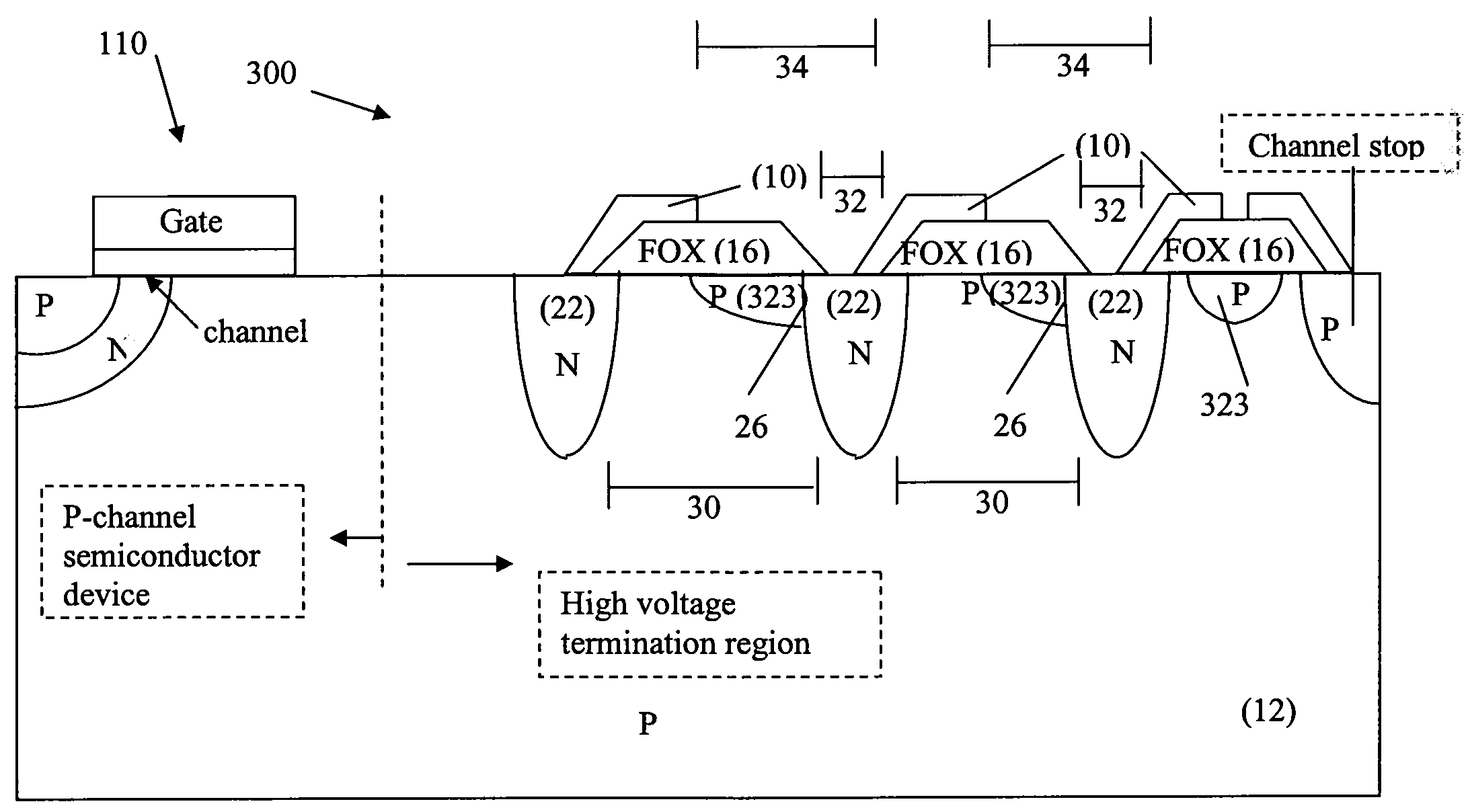
[0034]FIGS. 4A through 4E are cross-sectional views of different stages in the process of manufacturing a high-voltage termination structure (300) according to the present invention.

[0035]Referring to FIGS. 4A-4F, the first steps relating to the creation of the high-voltage termination structure (300), which may substantially surround a central active area (110), begin with a silicon wafer comprising a lightly-doped substrate (12) of a first semiconductor type, shown in the drawings as p-type.

[0036]The wafer is covered with a first photoresist, which can be selectively exposed to light and etched away, leaving a first photoresist mask and exposing a first surface of the substrate (12) in the high voltage termination structure (300) region.

[0037]Dopant may be implanted under the exposed first surface of the substrate (12), in the area of second termination regions (323), as shown in FIG. 4A. The implanted dopant may also be driven to form the second termination regions (323) of the f...


PUM


Abstract

High voltage semiconductor devices with high-voltage termination structures are constructed on lightly doped substrates. Lightly doped p-type substrates are particularly prone to depletion and inversion from positive charges, degrading the ability of associated termination structures to block high voltages. To improve the efficiency and stability of termination structures, second termination regions of the same dopant type as the substrate, more heavily doped than the substrate but more lightly doped than first termination regions, are positioned adjoining the first termination regions. The second termination regions raise the field threshold voltage where the surface is vulnerable and render the termination structure substantially insensitive to positive charges at the surface. The use of higher dopant concentration in the gap region without causing premature avalanche is facilitated by only creating second termination regions for regions lacking field plate protection.

Description

RELATED APPLICATION DATA[0001]This application claims the benefit of provisional application U.S. Ser. No. 60 / 973,345, filed Sep. 18, 2007, herein incorporated by reference.BACKGROUND OF THE INVENTION[0002]1. Technical Field[0003]The present invention relates to high-voltage semiconductor devices, and more particularly to improvements to termination structures associated with central active areas of high-voltage semiconductor devices.[0004]2. Discussion of Related Art[0005]In order to block high voltages, high voltage semiconductor devices are constructed on lightly doped semiconductor starting material. Due to the field effect, lightly doped p-type surfaces are particularly prone to depletion and inversion from positive charges abundantly present in dielectric films placed in contact with the surface to protect it from scratches or other mechanical damage. Regardless of the source of these positive charges, the field effect alters the effective spacing of the termination structure ...

Claims


Application Information

Patent Timeline
Patent Type & Authority Applications(United States)
IPC IPC(8): H01L29/06H01L21/76
CPCH01L21/761H01L29/0619H01L29/0638H01L29/7811H01L29/404H01L29/66712H01L29/0878
Inventor ZHANG, JINSHUSDRULLA, DUMITRUTSANG, DAH WEN
Owner MICROSEMI CORP ANALOG MIXED SIGNAL GRP LTD
Why Eureka
Try Eureka