Wafer inspecting sheet-like probe and application thereof

a wafer and probe technology, applied in the direction of individual semiconductor device testing, semiconductor/solid-state device testing/measurement, instruments, etc., can solve the problems of high inspection cost, long individual inspection time, and extremely expensive probe cards, and achieve the effect of retaining the inspection staggered

Inactive Publication Date: 2009-03-19
JSR CORPORATIOON
View PDF2 Cites 9 Cited by
  • Summary
  • Abstract
  • Description
  • Claims
  • Application Information

AI Technical Summary

Benefits of technology

[0036]Accordingly, a good electrically connected state to the wafer can be stably retained in inspection of the wafer.

Problems solved by technology

In the burn-in test on the other hand, it takes a long time to individually conduct burn-in test of a great number of integrated circuit devices because each integrated circuit device that is an object of inspection is fine, and its handling is inconvenient, whereby inspection cost becomes considerably high.
In order to produce a probe card used in such a probe test or WLBI test, it is however necessary to arrange a very great number of inspection probes, so that such a probe card is extremely expensive.
In addition, when the number of electrodes to be inspected is great, and the pitch thereof is fine, it is difficult to produce the probe card itself.
However, the above-described probe card involves the following problems.

Method used


Image

  • Wafer inspecting sheet-like probe and application thereof
  • Wafer inspecting sheet-like probe and application thereof
  • Wafer inspecting sheet-like probe and application thereof

Examples


Embodiment Construction

[0182]The embodiments of the present invention will hereinafter be described in detail.

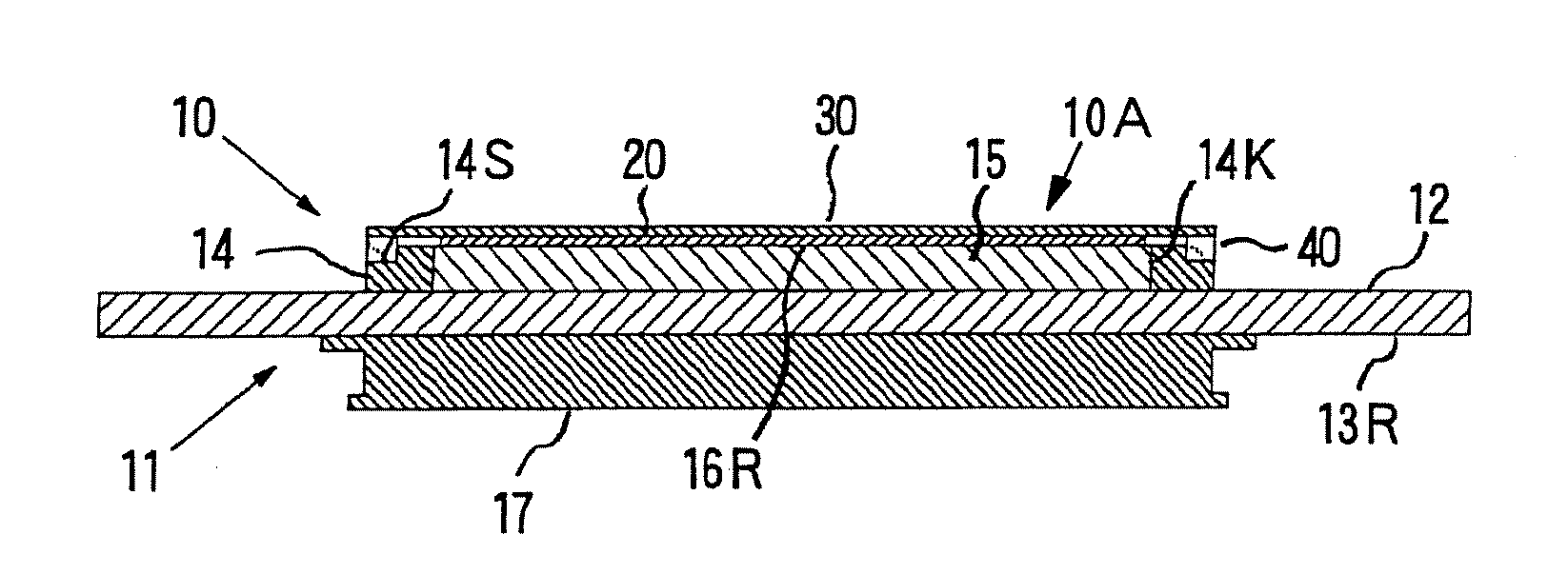
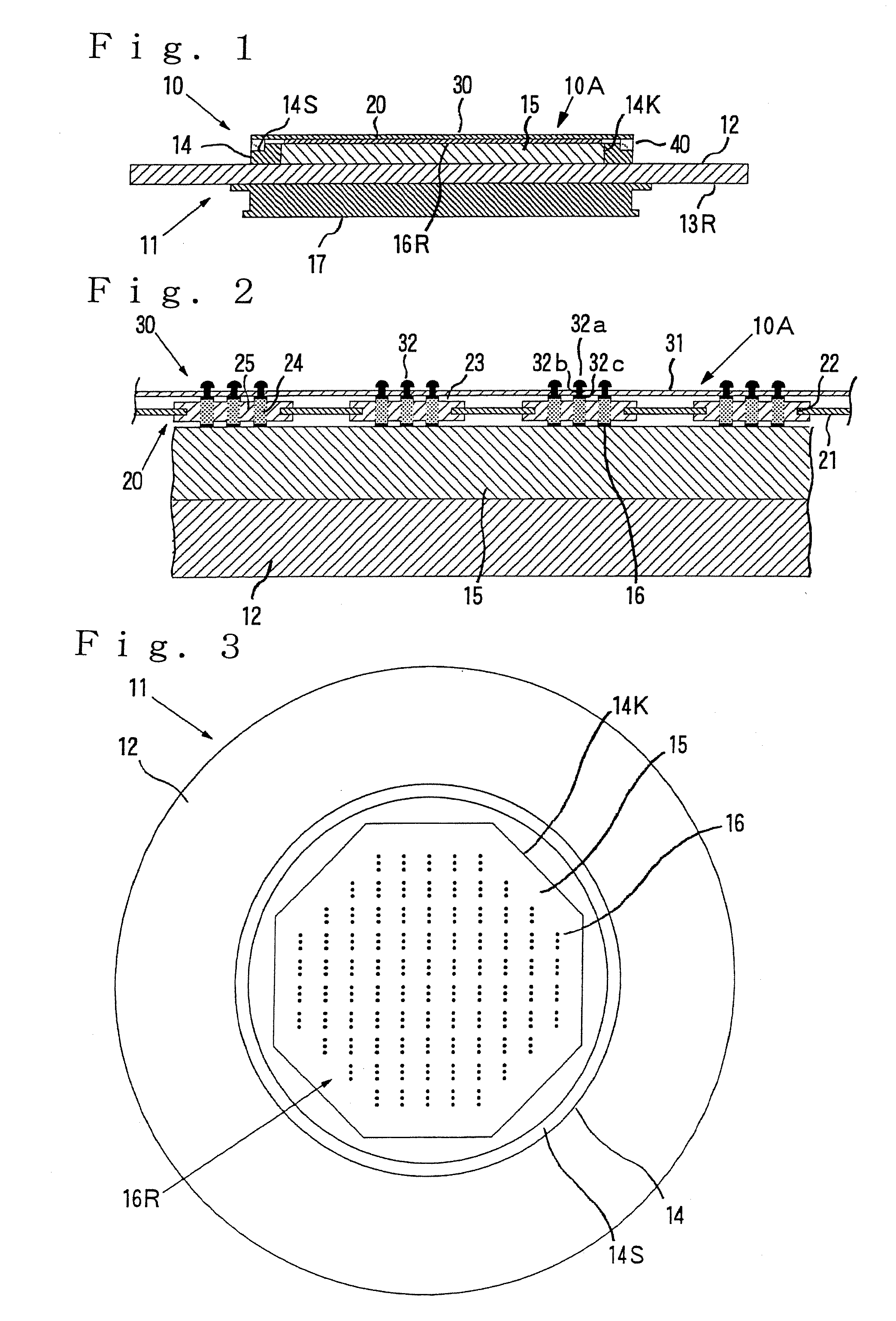
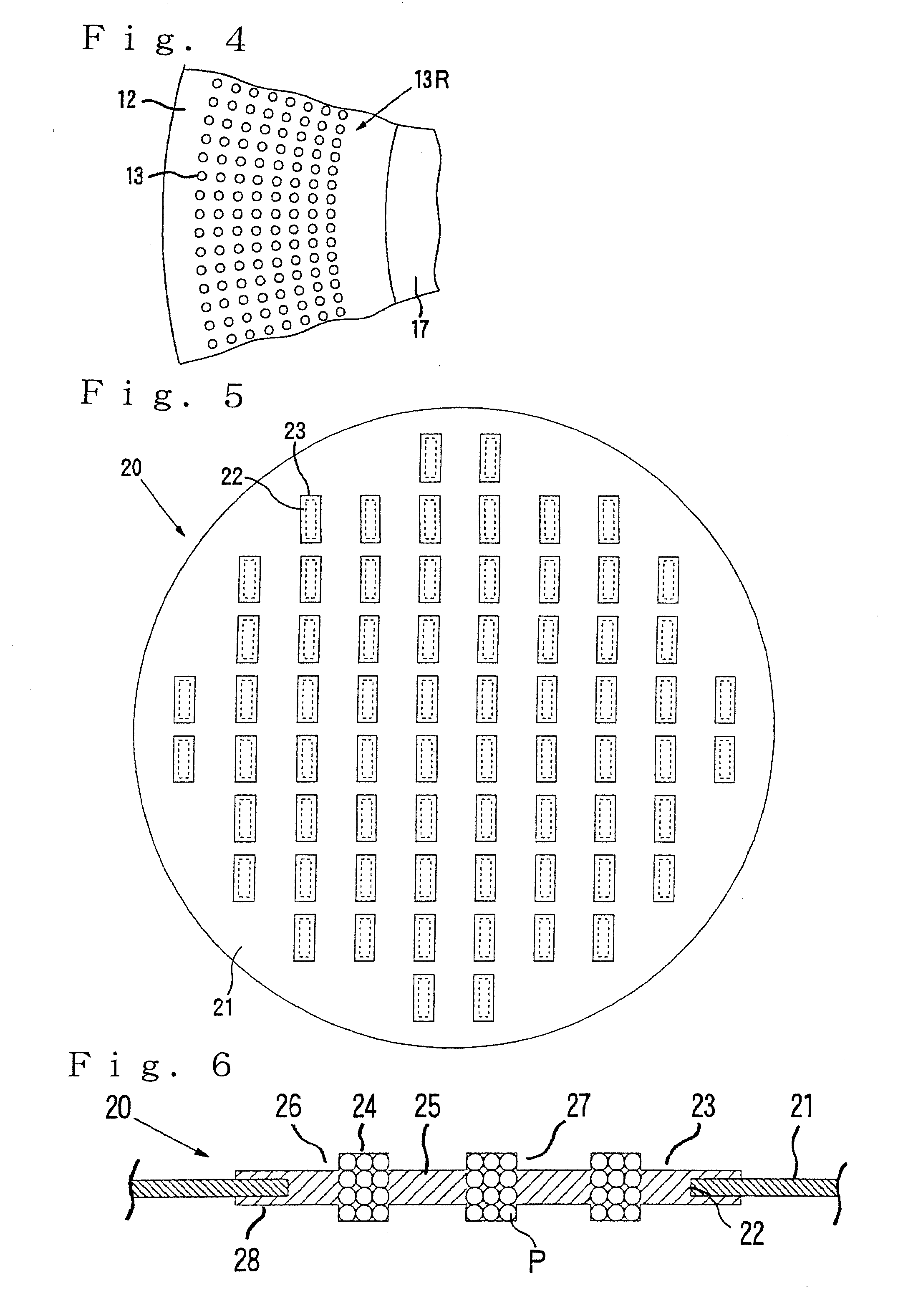
[0183]FIG. 1 is a cross-sectional view illustrating the construction of a first exemplary probe card for wafer inspection (hereinafter referred to as “probe card” merely) according to the present invention, and FIG. 2 is a cross-sectional view illustrating the construction of a principal part of the first exemplary probe card.

[0184]This first exemplary probe card 10 is used for collectively conducting a burn-in test on, for example, a wafer, on which a plurality of integrated circuits have been formed, as to each of the integrated circuits in a state of the wafer, and is constructed by a circuit board 11 for inspection and a probe member 10A for wafer inspection (hereinafter referred to as “probe member” merely), which is arranged on one surface (upper surface in FIG. 1 and FIG. 2) of this circuit board 11 for inspection, and the probe member 10A is constructed by a sheet-like probe 30 for wafer i...


PUM


Abstract

Disclosed herein are a sheet-like probe for wafer inspection, by which a good electrically connected state to a wafer can be surely achieved even when the pitch of electrodes to be inspected in the wafer is extremely small, and applications thereof.
The sheet-like probe for wafer inspection of the invention has an insulating sheet, in which a plurality of through-holes each extending in a thickness-wise direction of the insulating sheet have been formed in accordance with a pattern corresponding to a pattern of electrodes to be inspected in all or part of integrated circuits formed on a wafer, and electrode structures arranged in the respective through-holes in the insulating sheet so as to protrude from both surfaces of the insulating sheet. Each of the electrode structures is formed by linking a front-surface electrode part exposed to a front surface of the insulating sheet and having a diameter greater than a front surface-side opening diameter of the through-hole in the insulating sheet to a back-surface electrode part exposed to a back surface of the insulating sheet and having a diameter greater than a back surface-side opening diameter of the through-hole in the insulating sheet through a short circuit part inserted through into the through-hole in the insulating sheet, and is movable in the thickness-wise direction of the insulating sheet.

Description

TECHNICAL FIELD[0001]The present invention relates to a sheet-like probe for wafer inspection, a probe member for wafer inspection, a probe card for wafer inspection and a wafer inspection apparatus, which are suitable for use in conducting electrical inspection of a plurality of integrated circuits formed on a wafer in a state of the wafer.BACKGROUND ART[0002]In the production process of semiconductor integrated circuit devices, after a great number of integrated circuits are formed on a wafer composed of, for example, silicon, a probe test that basic electrical properties of each of these integrated circuits are inspected, thereby sorting defective integrated circuits is generally conducted. This wafer is then diced, thereby forming semiconductor chips. Such semiconductor chips are housed and sealed in respective proper packages. Each of the packaged semiconductor integrated circuit devices is further subjected to a burn-in test that electrical properties thereof are inspected und...

Claims


Application Information

Patent Timeline
Patent Type & Authority Applications(United States)
IPC IPC(8): G01R1/067
CPCG01R1/06711G01R3/00G01R1/0735H01L22/00
Inventor KIMURA, KIYOSHIHARA, FUJIOYAMADA, DAISUKE
Owner JSR CORPORATIOON
Why Eureka
Try Eureka