Method for manufacturing substrate

Active Publication Date: 2012-11-29
MURATA MFG CO LTD
View PDF3 Cites 3 Cited by
  • Summary
  • Abstract
  • Description
  • Claims
  • Application Information

AI Technical Summary

Benefits of technology

[0014]According to a preferred embodiment of the present invention, the metal bump formed on the metal foil conductor which is to be contact-bonded to the thermosetting insulating resin is subjected to a heating treatment at a low temperature, thereby making it possible to cause the metal fillers of the bump bound to each other by melting, and cause a metallic bond formed by diffusion in the solid layer between the bump and the metal foil, thereby providing a favorable electrical connection between the metal foil and the metal column of the bump. Then, the metal column is press-fitted into the uncured or semi-cured insulating resin layer before being completely cured, thereby contact-bonding the metal foil to the insulating resin layer and joining the tip of the metal column to the opposed metallic member inside or outside the insulating resin layer, and the insulating resin layer is then subjected to a heat treatment to reheat the metal column, thereby making it possible to re-melt the metal fillers of the metal column, and form a metallic bond between the metal column and the metallic member by alloying through diffusion in the solid layer, thus providing a highly favorable electrical connection between the metal foil and the metallic member.
[0015]In this case, the metal foil contact-bonded to the insulating layer and the metallic member are electrically connected quite tightly by a metallic bond of alloying through diffusion in the solid layer between the metal bump integrally with the metal foil, which is press-fitted into the insulating resin layer from one main principal surface thereof, and the metallic member, rather than being connected by metal bumps in physical contact with each other, which are press-fitted from both principal surfaces of an insulating resin layer to be opposed to each other, as in a conventional case. Thus, the reliability of the electrical connection is improved spectacularly.
[0016]According to a preferred embodiment of the present invention, the metal bump is formed on the metal foil on one principal surface of the insulating resin layer, heated at a low temperature to be integrated, and then

Problems solved by technology

In this case, when the metal columns are to be formed with the use of vias, the insulating resin layer requires the use of hole-forming processing, plating processing, etc., which make the manufacturing process complicated, and thus expensive, which is further also disadvantageous in that

Method used


Image

  • Method for manufacturing substrate
  • Method for manufacturing substrate
  • Method for manufacturing substrate

Examples


first preferred embodiment

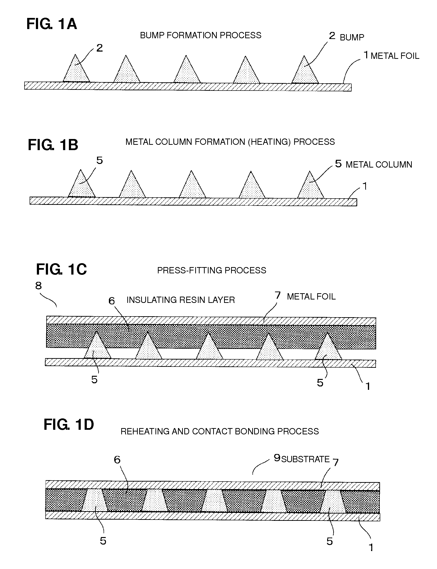
[0031]First, a first preferred embodiment of the present invention will be described with reference to FIGS. 1A to 4.

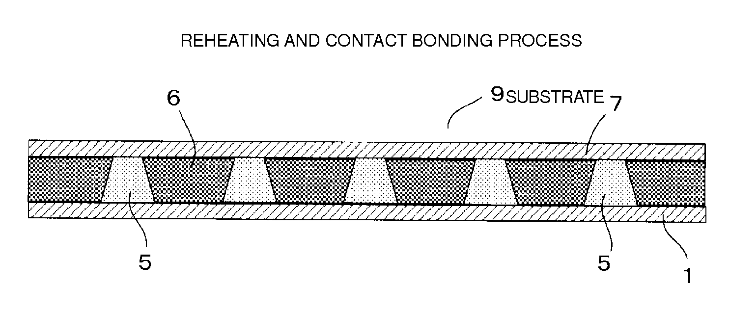
[0032]FIGS. 1A-1D show a method for manufacturing a substrate according to the present preferred embodiment in process sequence.

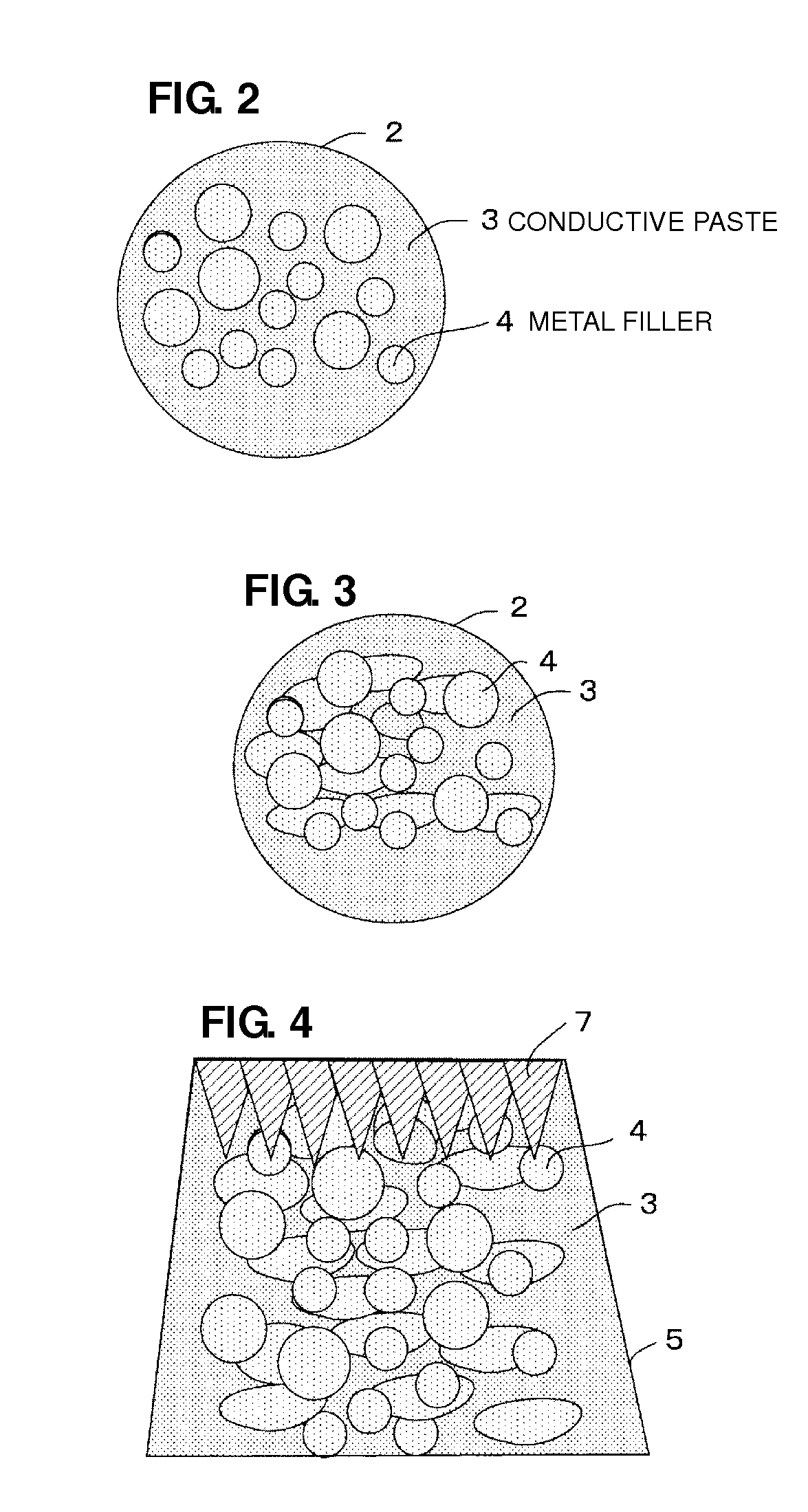
[0033]In a first bump formation step (FIG. 1A), one metal foil 1 is prepared as a carrier contact-bonded to one principal surface of a thermosetting insulating resin layer formed from an epoxy resin or other suitable material as will be described later, and bumps 2 of a conductive paste including metal fillers which can be melted at a temperature lower than the curing temperature (around 180° C.) of the insulating resin layer are formed on the surface of the metal foil 1. FIG. 2 shows a transverse section of the bump 2 in a bump formation process (before heating), and particles of metal fillers 4 are scattered substantially homogeneously in a conductive paste 3 in the bump 2 before heating.

[0034]The metal foil 1 may be fundamentally various t...

second preferred embodiment

[0047]Next, a second preferred embodiment of the present invention will be described with reference to FIGS. 5A and 5B.

[0048]In the case of the present preferred embodiment, the metal columns 5 integrally connected to the metal foil 1 in FIG. 1B are preferably formed on, for example, a transfer plate (not shown) according to the bump formation step and metal column formation in the first preferred embodiment.

[0049]Next, an insulating resin layer 10 with components built therein is prepared in a press-fitting process in FIG. 5A in place of the press-fitting process in FIG. 1C. The insulating resin layer 10 is formed, for example, by burying one or more electronic components 11 such as coils, capacitors, transistors, and ICs in the uncured resin layer 6 according to the first preferred embodiment, and a wiring pattern of a metal foil 12 corresponding to the metal foil 7 in FIG. 1C is contact-bonded to the lower surface of the insulating resin layer 10. The electronic components 11 hav...

modification example

[0054]Incidentally, the metal columns 5 preferably have a larger area of the base on the metal foil 1 side, and have contact with the external electrodes 11a in a straddling and protruding manner. FIG. 6 shows the metal columns 5 in contact with external the electrodes 11a in a straddling and protruding manner through the press-fitting process.

[0055]More specifically, in the case of providing connections through conventional vias, processing down to the bottom has to be carried out without damaging external electrodes. Thus, via processing itself is difficult, and it is thus difficult to control the processing conditions. In addition, the variation in component height, the variation in mounting, etc., cause a failure to control the thickness of the insulating resin layer 10 on the external electrodes 11a, thereby causing defective processing.

[0056]Furthermore, in the case of the metal columns 5 in FIGS. 5A and 5B, the projected area of the metal column 5 viewed from above is smaller...


PUM

PropertyMeasurementUnit
Currentaaaaaaaaaa
Currentaaaaaaaaaa
Luminous intensityaaaaaaaaaa

Abstract

In a method for manufacturing a substrate, connections are provided through metal columns of bumps press-fitted into an insulating resin layer between metal foils contact-bonded to a thermosetting insulating resin layer. Bumps of a conductive paste containing metal fillers are formed on a metal foil which is to be contact-bonded to an insulating resin layer, the bumps are heated to bound the metal fillers to each other, and form a metallic bond between the bumps and the metal foil, the metal columns are press-fitted into the insulating resin layer to contact-bond the metal foil to the insulating resin layer, and join the tips of the metal columns to a metal foil, the metal columns are then reheated to form a metallic bond between the metal columns and the metal foil.

Description

BACKGROUND OF THE INVENTION[0001]1. Field of the Invention[0002]The present invention relates to a method for manufacturing a substrate, in which metal columns of bumps press-fitted into an insulating resin layer provide connections between metal foils contact-bonded to a thermosetting insulating resin layer, or between a metal foil contact-bonded to a thermosetting insulating resin layer and an electrode of an electronic component built in the insulating resin layer, and more particularly relates to an improvement in reliability of an electrical connection.[0003]2. Description of the Related Art[0004]In general, double-sided wiring boards and multilayer wiring substrates are manufactured by connecting a wiring pattern of a metal foil on one principal surface of an insulating resin layer (organic resin layer) and a wiring pattern of a metal foil on the other principal surface thereof to each other through the use of metal columns penetrating through the insulating resin layer. In th...

Claims


Application Information

Patent Timeline
IPC IPC(8): B23K31/02
CPCH05K1/185H05K3/4069H05K3/4617H05K2203/1189H05K3/4652H05K2201/0355H05K3/4647
Inventor SEKIMOTO, YASUYUKI
Owner MURATA MFG CO LTD
Why Eureka
Try Eureka