

Array substrate and method of manufacturing the same, display panel and method of manufacturing the same, and display device
- Summary
- Abstract
- Description
- Claims
- Application Information
AI Technical Summary
Benefits of technology
Problems solved by technology
Method used
Image

Examples
Embodiment Construction
[0061]In order to make clearer understanding of the above objects, features and advantages of the present disclosure, the present invention will be described hereinafter in detail with reference to exemplary embodiments and attached drawings. It is noted that in case of no conflict, the embodiments of the present disclosure and features thereof may be combined.
[0062]In the following detailed description, for purposes of explanation, numerous specific details are set forth in order to provide a thorough understanding of the disclosed embodiments. It will be apparent, however, the present invention may be embodied in many different forms and should not be construed as being limited to the embodiment set forth herein; rather, these embodiments are provided so that the present invention will be thorough and complete, and will fully convey the concept of the disclosure to those skilled in the art.
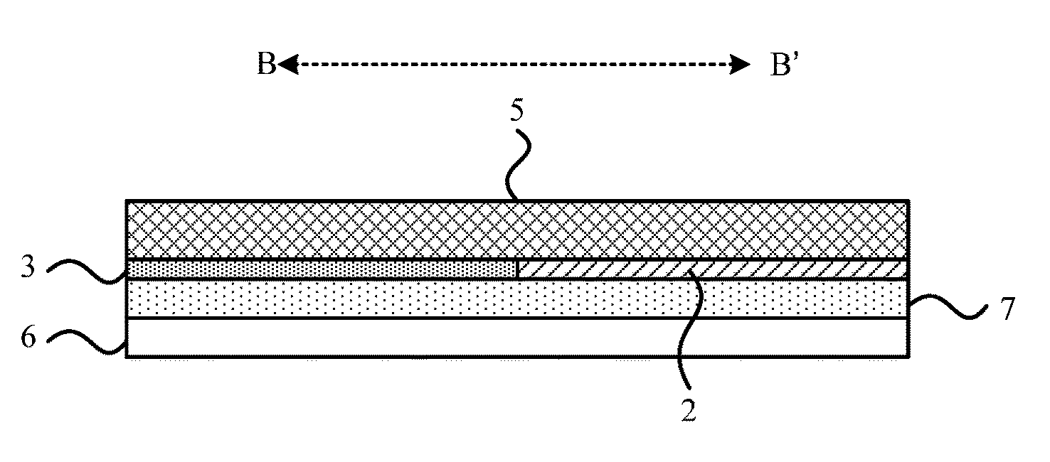
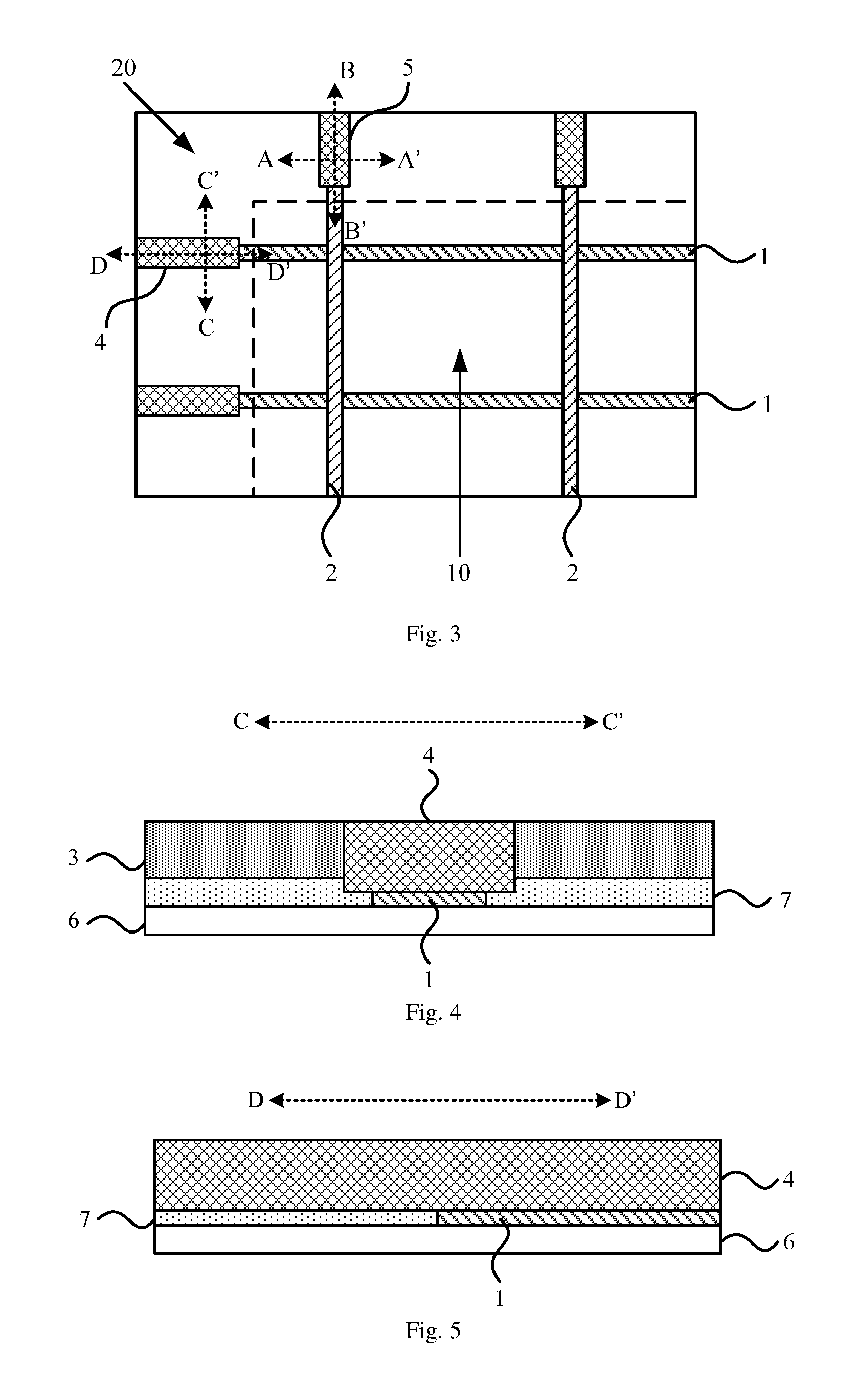
[0063]An array substrate according to an embodiment of the present disclosure, as shown in F...
PUM
 Abstract
Description
Claims
Application Information