Light emitting/receiving element

a technology of light emitting and receiving elements, applied in the direction of diodes, electric discharge tubes, semiconductor devices, etc., can solve the problem that the apparatus cannot be easily produced, and achieve the effect of easy production

Inactive Publication Date: 2009-03-26
FUJIFILM CORP
View PDF9 Cites 27 Cited by
  • Summary
  • Abstract
  • Description
  • Claims
  • Application Information

AI Technical Summary

Benefits of technology

[0005]The invention has been conducted under the above-discussed circumstances. It is an object of the invention to provide a light emitting / receiving element and imaging device which have both the function of a light receiving element and that of a light emitting element, and which can be easily produced.
[0015]According to the first aspect of the invention, it is possible to provide a light emitting / receiving element which has both the function of a light receiving element and that of a light emitting element, and which can be easily produced.
[0024]According to the second aspect of the invention, it is possible to provide an imaging apparatus which has both the function of a light receiving element and that of a light emitting element, and which can be easily produced.
[0035]According to the third aspect of the invention, it is possible to provide an imaging device which has both the function of a light receiving element and that of a light emitting element, and which can be easily produced.

Problems solved by technology

Therefore, film formation and patterning of the light emitting layers, and those of the photoelectric converting layers must be separately conducted, with the result that the apparatus cannot be easily produced.

Method used


Image

  • Light emitting/receiving element
  • Light emitting/receiving element
  • Light emitting/receiving element

Examples


first embodiment

[0129]FIG. 15 is a partial sectional diagram schematically showing the configuration of an imaging device of a first embodiment of the invention.

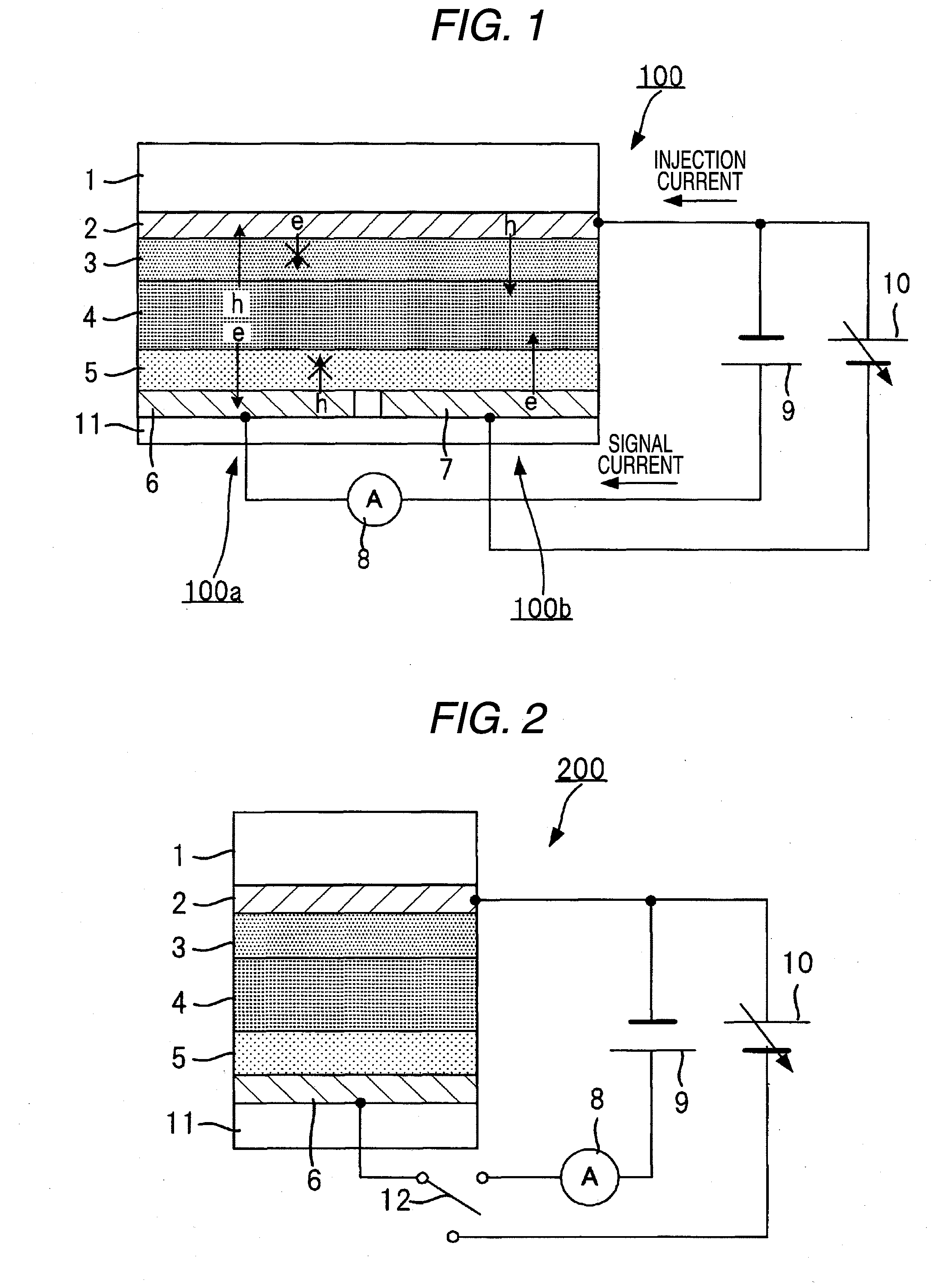
[0130]The imaging device 100Y shown in FIG. 15 includes: a substrate 1Y such as a glass substrate or a semiconductor substrate; an insulating layer 2Y which is formed on the substrate 1Y; a plurality of pixel electrodes 3Y which are arranged one- or two-dimensionally on the insulating layer 2Y; a photoelectric converting layer 4Y which is formed on the pixel electrodes 3Y; an opposing electrode 5Y which is formed on the photoelectric converting layer 4Y; an insulating layer 6Y which is formed on the opposing electrode 5Y; a light emitting element 16Y consisting of a transparent electrode 7Y which is formed on the insulating layer 6Y, a light emitting layer 8Y which is formed on the transparent electrode 7Y, and a transparent electrode 9Y which is formed on the light emitting layer 8Y; a protective layer 10Y which is formed on the transparen...

second embodiment

[0164]FIG. 19 is a partial sectional diagram schematically showing the configuration of an imaging device of a second embodiment of the third aspect of the invention.

[0165]In FIG. 19, components which are similar in configuration to those of FIG. 15 are denoted by the same reference numerals.

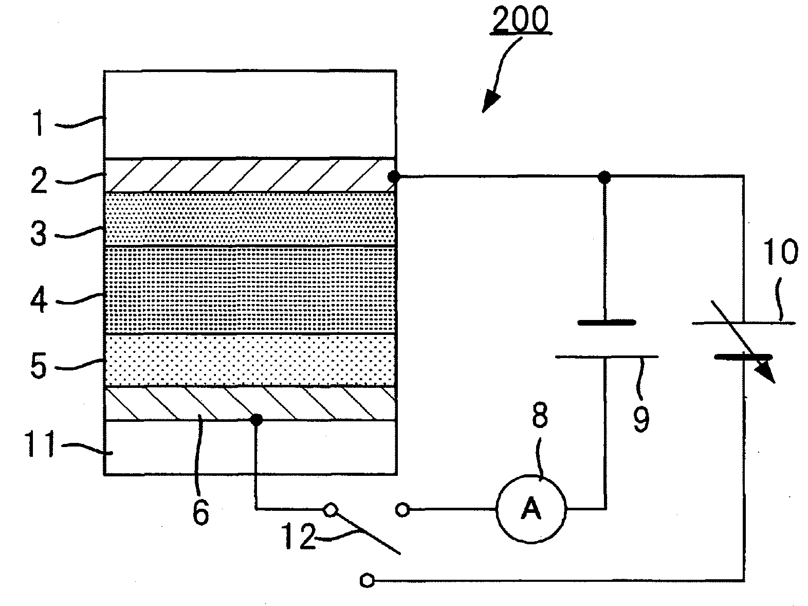
[0166]The imaging device 200Y shown in FIG. 19 has a configuration where the opposing electrode 5Y of the imaging device 100Y shown in FIG. 15 functions also as the transparent electrode 7Y so as to omit the light emitting electrode 7Y and the insulating layer 6Y. According to the configuration, the number of wirings from the power supplies 13Y, 14Y, the thickness of the imaging device 200Y, and the loss of light incident on the photoelectric converting layer 4Y can be suppressed.

third embodiment

[0167]FIG. 20 is a partial sectional diagram schematically showing the configuration of an imaging device of a third embodiment of the third aspect of the invention.

[0168]In FIG. 20, components which are similar in configuration to those of FIG. 19 are denoted by the same reference numerals.

[0169]The imaging device 300Y shown in FIG. 20 has a configuration where an electron blocking layer 26Y is disposed between the functional layer 3Y of the imaging device 200Y shown in FIG. 19 and the photoelectric converting layer 4Y, a hole blocking layer 17Y is disposed between the photoelectric converting layer 4Y and the opposing electrode 5Y, an electron transporting layer 18Y is disposed between the opposing electrode 5Y and the light emitting layer 8Y, and a hole transporting layer 19Y is disposed between the light emitting layer 8Y and the transparent electrode 9Y.

[0170]According to the configuration, injection of holes from the opposing electrode 5Y to the photoelectric converting layer ...


PUM


Abstract

A light emitting / receiving element includes: a substrate; an organic layer which is provided above the substrate; a forward bias power supply which applies a bias voltage between both ends of the organic layer so as to inject charges from an outside into the organic layer; a reverse bias power supply which applies a bias voltage, which is opposite in polarity to the bias voltage applied by the forward bias power supply, between the both ends of the organic layer so as to extract charges generated in the organic layer to the outside; and a current detecting unit, wherein the organic layer includes an organic material which, when the bias voltage is applied by the forward bias power supply, has the light emitting function, and which, when the bias voltage is applied by the reverse bias power supply, has the photoelectric converting function.

Description

CROSS-REFERENCE TO RELATED APPLICATIONS[0001]This application claims the benefit of Japanese Patent Application JP 2007-249917, filed Sep. 26, 2007, Japanese Patent Application JP 2007-249918, filed Sep. 26, 2007, and Japanese Patent Application JP 2007-249919, filed Sep. 26, 2007, the entire contents of which are hereby incorporated by reference, the same as if set forth at length.FIELD OF THE INVENTION[0002]The present invention relates to a light emitting / receiving element having a light emitting function, and a photoelectric converting function of converting received light to charges, and also to an imaging apparatus having a photoelectric converting function of converting light from an object to charges, and an illuminating function of illuminating the object.BACKGROUND OF THE INVENTION[0003]Conventionally, an imaging apparatus in which light emitting elements and light receiving elements are mixedly used has been proposed (see JP-A-2007-104088 (corresponding to US2007 / 0077105A...

Claims


Application Information

Patent Timeline
Patent Type & Authority Applications(United States)
IPC IPC(8): H01J40/00
CPCH01L27/3234H01L51/5203H01L27/3244H10K65/00H10K59/12H10K39/34H10K59/805H10K50/805H10K59/65
Inventor INUIYA, MASAFUMI
Owner FUJIFILM CORP
Why Eureka
Try Eureka