
Integrated capacitive sensing devices and methods

a capacitive sensing and integrated technology, applied in the field of touch screen display devices, can solve the problems of reducing display brightness, reducing user experience, and reducing display size, so as to improve user experience, reduce brightness, and reduce thickness

Inactive Publication Date: 2009-03-26
MOTOROLA MOBILITY LLC
View PDF5 Cites 66 Cited by
  • Summary
  • Abstract
  • Description
  • Claims
  • Application Information

AI Technical Summary

Benefits of technology

"The patent text discusses the trend towards smaller mobile communication devices and the desire to add more features without adding too many hardware components. However, traditional touch screens are often thick and can negatively impact the device's aesthetics. The patent proposes a solution using integrated photosensors in the thin film transistor liquid crystal display (TFT) array or internal cell gap capacitive sensing to achieve a thinner design with improved sensitivity and resolution."

Problems solved by technology

As mobile communication device technology has continued to improve, the devices have become increasingly smaller and thinner.
Moreover, in resistive designs, spacers are usually visible as well, detracting from aesthetics of the device.
Such an implementation significantly reduces the display brightness due to pixel aperture ratio reduction and requires a complicated sensing algorithm as well as restrictive color schemes.
Additionally, integrated photosensors in the TFT array can only sense one touch point at a time.
Again, with this implementation, there is a significant reduction in display brightness as well as a limited resolution.

Method used


Image

  • Integrated capacitive sensing devices and methods
  • Integrated capacitive sensing devices and methods
  • Integrated capacitive sensing devices and methods

Examples


Embodiment Construction

[0011]It would be beneficial, in a thin design touch screen, in particular, to avoid a reduction in display brightness. It would be further beneficial to include fewer hardware and software components when adding new features and making improvements to the current features in the smaller and thinner devices. In particular, it is beneficial to reuse components that are already part of a device, possibly with a minimum of additional hardware or software components so that the device size and / or complexity is not substantially increased.

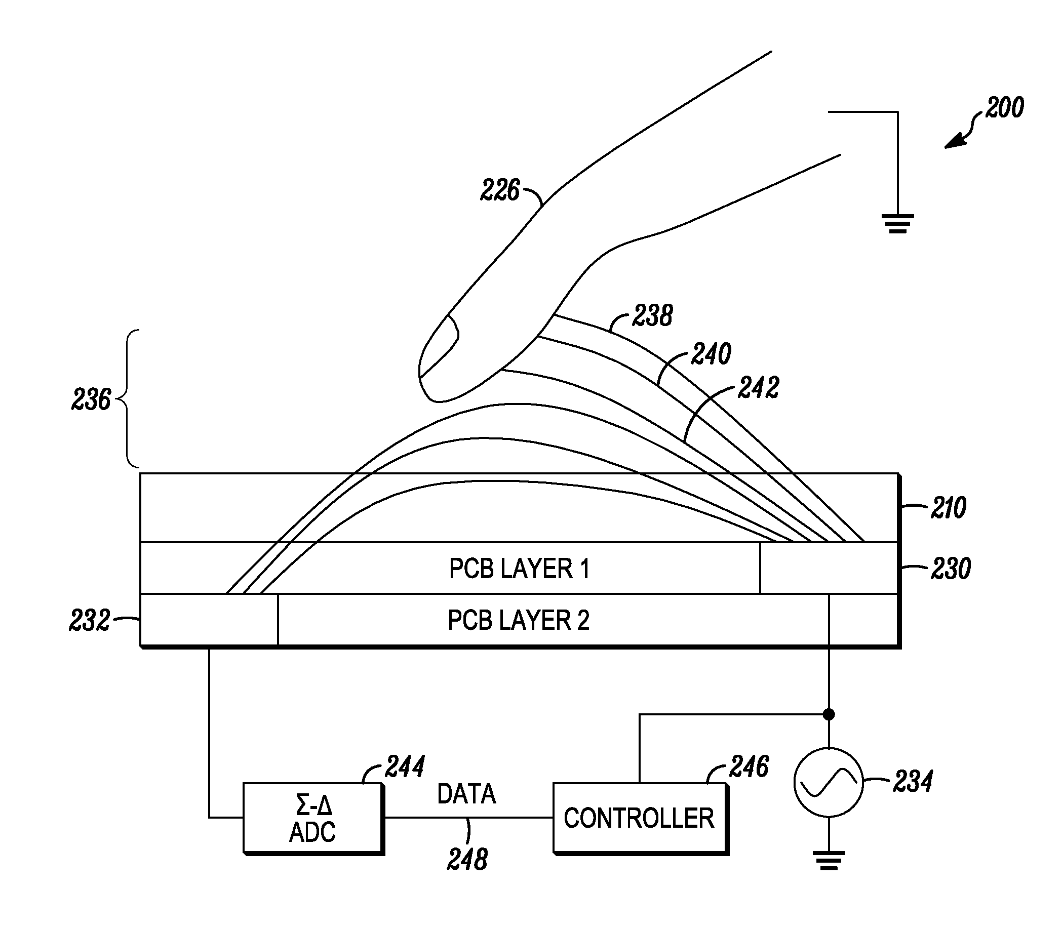
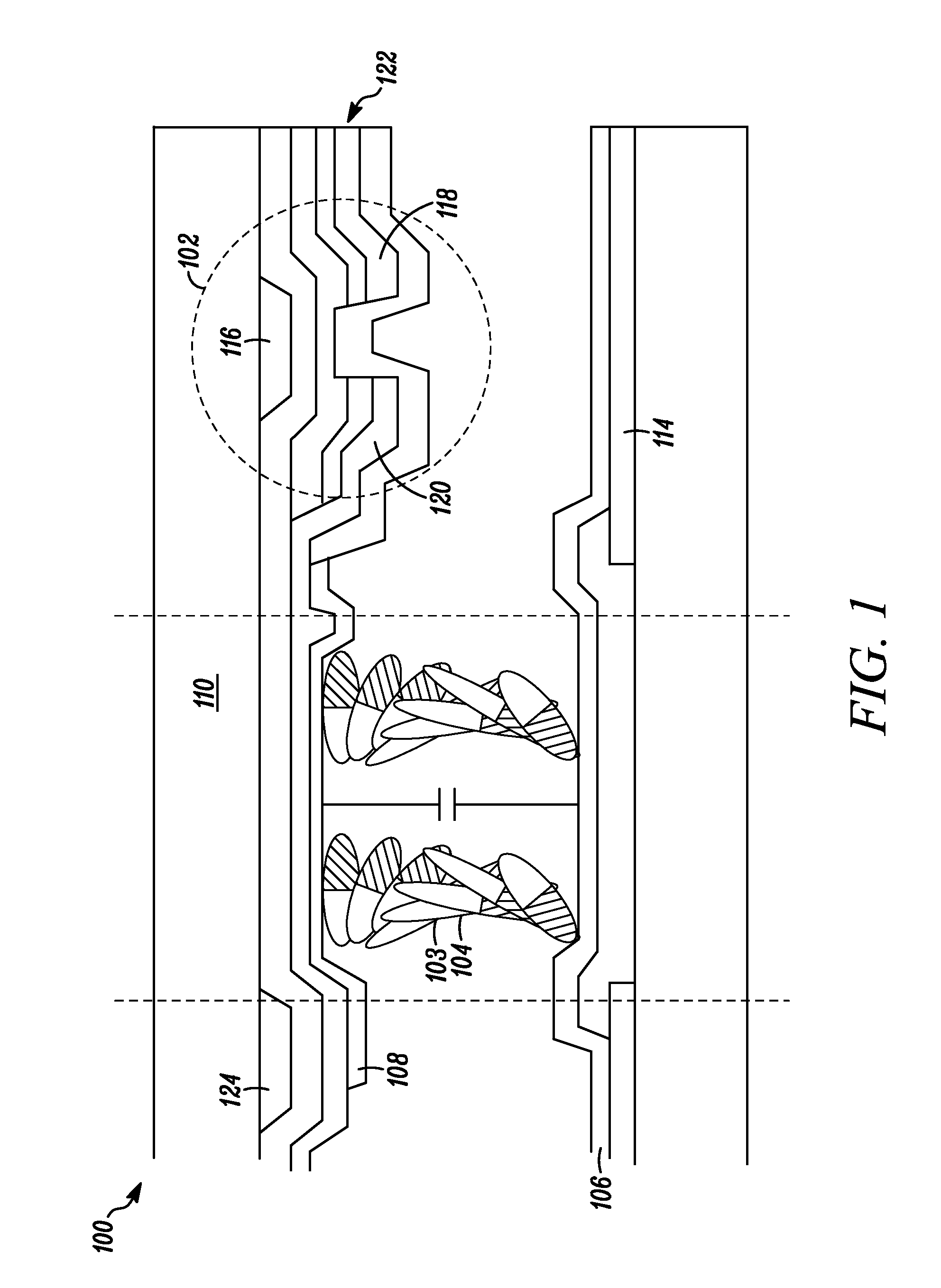
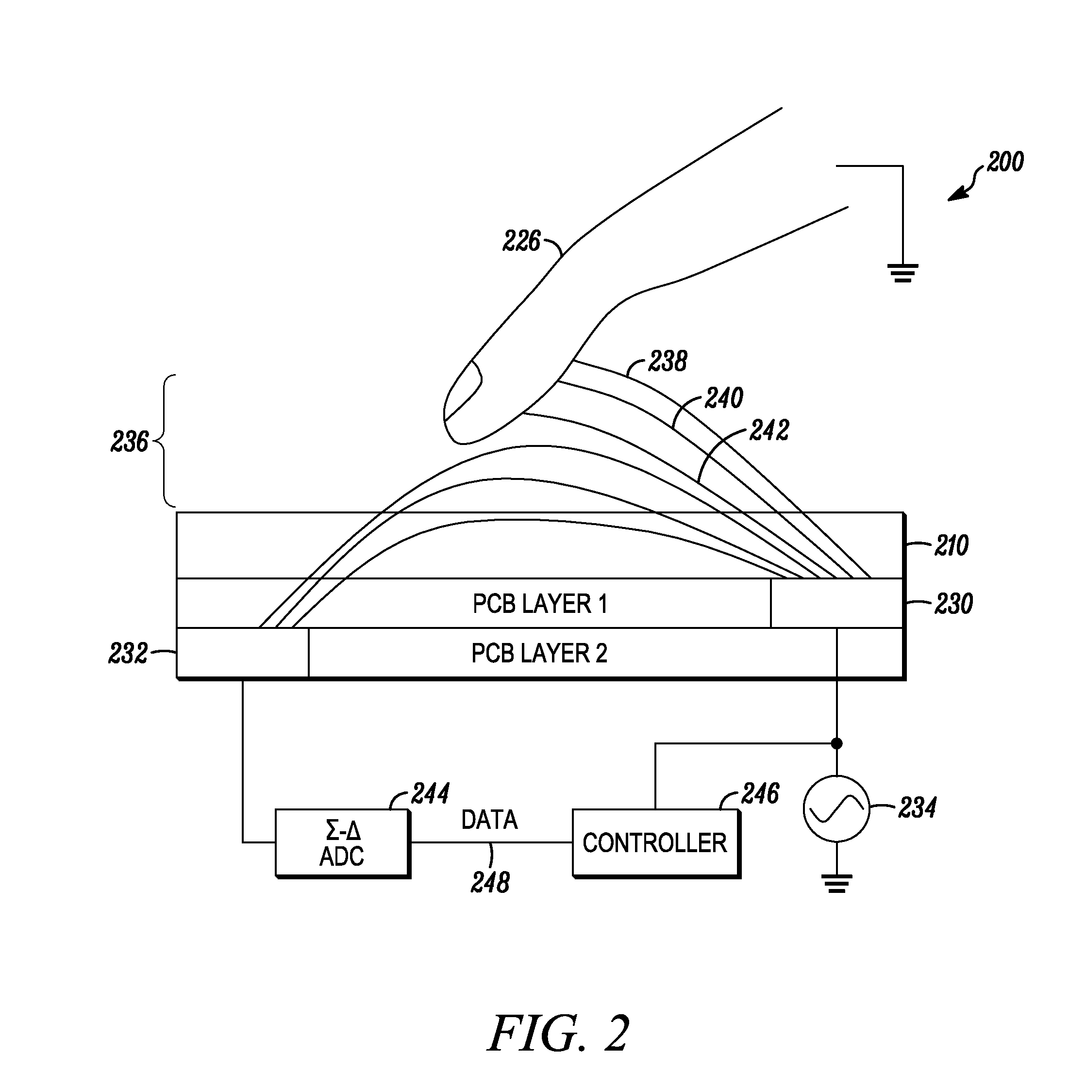
[0012]Disclosed are touch screen devices and methods of sensing an object near the surface of a touch screen device. As will be described in detail below, a capacitive sensor is integrated into display electronics by flipping the traditional thin film transistor liquid crystal display (TFT) stack-up which has a bottom gate structure so that as will be described in detail below, the TFT is an inverted bottom gate structure, that is, the gate faces outwar...


PUM


Abstract

Disclosed are touch screen devices and methods of sensing an object near the surface of a touch screen device. A capacitive sensor is integrated into display electronics by flipping the traditional thin film transistor liquid crystal display (TFT) stack-up which has a bottom gate structure so that it is an inverted bottom gate structure. Accordingly, the gate structure is near the top of the display and the gate drive lines are re-used as excitation lines in addition to their function as display lines. The excitation lines therefore drive excitation to generate an induced electric field at the surface of the display device. Additionally, other lines are used as sensor lines so that sensor signals are input to the device controller to determine the position of an object at the surface of the display device. Accordingly, the excitation lines are scanned to detect the presence of a finger or other object.

Description

FIELD[0001]Disclosed is a touch screen display device, and more particularly, integrated capacitive sensing devices and methods of an inverted bottom gate structure thin film transistor liquid crystal display to induce an electric field at the surface of the device and sense lines to detect shunted electric field lines to determine position of an object at the surface.BRIEF DESCRIPTION[0002]The makers of mobile communication devices, including those of cellular telephones, are increasingly adding functionality to their devices. While there is a trend toward the inclusion of more features and improvements for current features, there is also a trend toward smaller mobile communication devices. As mobile communication device technology has continued to improve, the devices have become increasingly smaller and thinner. Fewer and / or smaller hardware and software components are therefore desirable when adding new features and making improvements to the current features in the smaller devi...

Claims


Application Information

Patent Timeline
Patent Type & Authority Applications(United States)
IPC IPC(8): G06F3/041
CPCG06F3/044G06F3/0412G06F3/04166G06F3/0446G06F2203/04101G06F2203/04108G06F2203/04111G06F3/04164
Inventor KAEHLER, JOHN W.FOO, KEN K.ZHUANG, ZHIMING
Owner MOTOROLA MOBILITY LLC
Learn More