Reactor for polycrystalline silicon and polycrystalline silicon production method

a polycrystalline silicon and production method technology, applied in the direction of crystal growth process, after-treatment details, silicon compounds, etc., can solve the problems of undesirable morphology at the lower part of the produced column-shaped polycrystalline, difficult to supply raw material gas to the lower part, etc., to prevent undesirable morphology of polycrystalline silicon and stable supply of raw material gas

Active Publication Date: 2009-03-26
HIGH-PURITY SILICON CORP
View PDF3 Cites 14 Cited by
  • Summary
  • Abstract
  • Description
  • Claims
  • Application Information

AI Technical Summary

Benefits of technology

[0021]According to the reactor for polycrystalline silicon of the present invention, it is possible to stably supply a raw material gas to the surface of a silicon seed rod and prevent polycrystalline silicon from formation of undesirable morphology.

Problems solved by technology

In this instance, when the upper end of the raw material gas supply nozzle extending upward is set to a height greater than +5 cm on the basis of the upper end of the electrode retaining the silicon seed rod, the raw material gas is difficult to supply to the lower part of the silicon seed rod, and there is a concern that undesirable morphology may take place at the lower part of the produced column-shaped polycrystalline silicon.

Method used


Image

  • Reactor for polycrystalline silicon and polycrystalline silicon production method
  • Reactor for polycrystalline silicon and polycrystalline silicon production method
  • Reactor for polycrystalline silicon and polycrystalline silicon production method

Examples


Embodiment Construction

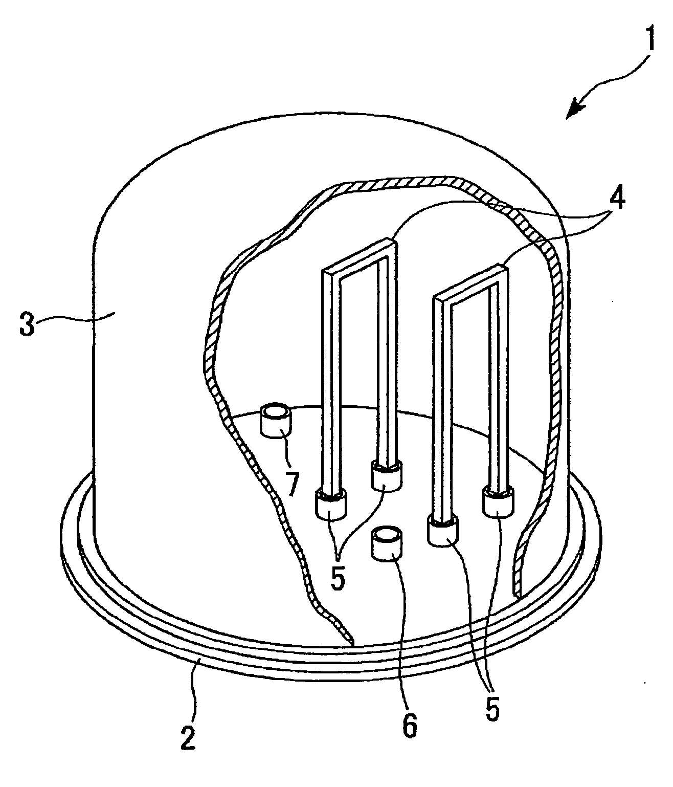
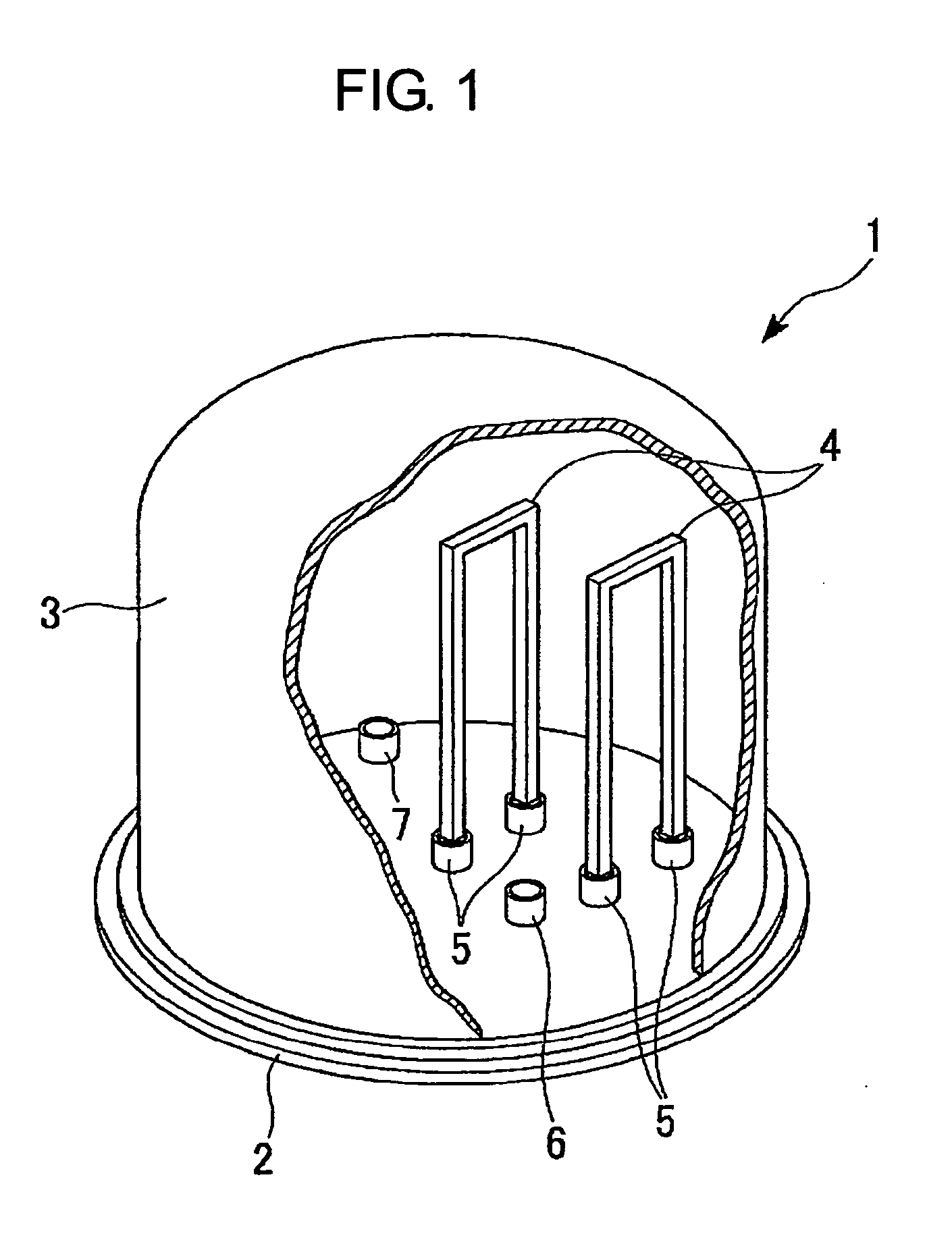
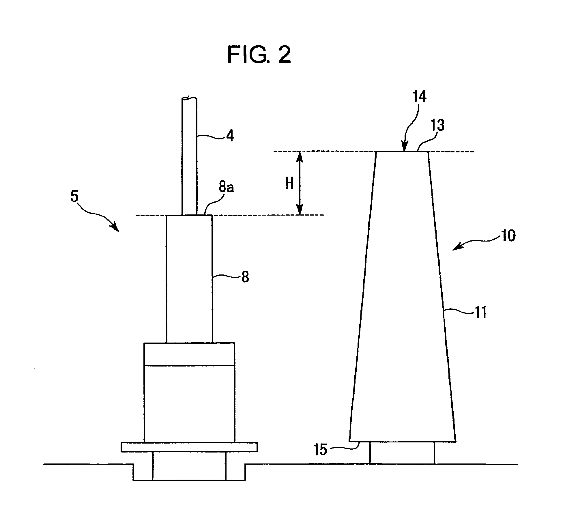
[0026]Hereinafter, an explanation will be made of a reactor for polycrystalline silicon which is an embodiment of the present invention by referring to drawings. FIG. 1 is a schematic pattern diagram of the reactor for polycrystalline silicon. FIG. 2 is a side elevational view showing a raw material gas supply nozzle and an electrode used in the reactor for polycrystalline silicon. FIG. 3 is a longitudinal sectional view of the raw material gas supply nozzle.

[0027]As shown in FIG. 1, the reactor for polycrystalline silicon 1 of the present embodiment is provided with a bell jar 3 formed in a bell shape so as to cover entirely a space above the bottom of the reactor2 mounted in a circular shape. The interior of the reactor for polycrystalline silicon 1 is sealed hermetically by the bottom of the reactor 2 and the bell jar 3. A plurality of silicon seed rods 4 which are formed approximately in a n-shape, with the upper ends being connected to each other, and serving as a seed rod of t...


PUM

PropertyMeasurementUnit
heightaaaaaaaaaa
heightaaaaaaaaaa
temperatureaaaaaaaaaa

Abstract

The reactor for polycrystalline silicon is a reactor for polycrystalline silicon in which a silicon seed rod installed inside the reactor is heated by supplying electricity, a raw material gas supplied inside the reactor is allowed to react, thereby producing polycrystalline silicon on the surface of the silicon seed rod, and specifically, the reactor for polycrystalline silicon is provided with a raw material gas supply port installed on the bottom of the reactor and a raw material gas supply nozzle attached to the raw material gas supply port so as to be communicatively connected and extending upward, in which the upper end of the raw material gas supply nozzle is set to a height in a range from −10 cm to +5 cm on the basis of the upper end of the electrode which retains the silicon seed rod.

Description

CROSS-REFERENCE TO RELATED APPLICATIONS[0001]This application claims priority to Japanese Patent Application No. 2007-244352 filed on Sep. 20, 2007, and Japanese Patent Application No. 2008-177980 filed on Jul. 8, 2008, the contents of which are incorporated herein by reference.BACKGROUND OF THE INVENTION[0002]1. Field of the Invention[0003]The present invention relates to a reactor for polycrystalline silicon used in producing polycrystalline silicon according to the Siemens method, and relates to a polycrystalline silicon production method.[0004]2. Description of Related Art[0005]The Siemens method is known as a method for producing polycrystalline silicon of high purity used as a material of semiconductors. In the Siemens method, a raw material gas composed of chlorosilane and hydrogen is brought into contact with a heated silicon seed rod to deposit polycrystalline silicon on the surface through reactions of the raw material gas. A reactor for polycrystalline silicon in which ma...

Claims


Application Information

Patent Timeline
Patent Type & Authority Applications(United States)
IPC IPC(8): C23C16/24B05D3/14
CPCC01B33/035B01J2219/00247Y10T117/10B01J19/26B01J2219/00135C30B28/12
Inventor ENDOH, TOSHIHIDEISHII, TOSHIYUKISAKAGUCHI, MASAAKIHATAKEYAMA, NAOKI
Owner HIGH-PURITY SILICON CORP
Why Eureka
Try Eureka