Faceted ceramic fibers, tapes or ribbons and epitaxial devices therefrom

a technology of ceramic fibers and faceted ceramics, applied in the direction of superconductor devices, natural mineral layered products, superconductor fluids, etc., can solve the problems of ac loss, ac loss is generally high, substrates are also rigid and not flexible, etc., to achieve the effect of reducing ac loss and reducing ac loss

Inactive Publication Date: 2009-03-26
UT BATTELLE LLC
View PDF67 Cites 44 Cited by
  • Summary
  • Abstract
  • Description
  • Claims
  • Application Information

AI Technical Summary

Benefits of technology

[0022]The method can further comprise the step of twisting the fiber, tape or ribbon for reduction of AC losses, or transposing or braiding two or more of fibers, tapes or ribbons for reduction of AC losses.

Problems solved by technology

However, these substrates cannot be fabricated using known processes in long lengths or in large areas and are generally limited to sizes of no more than about a foot in length and diameter.
These substrates are also rigid and not flexible because these substrates are typically at least about 1 mm thick.
However, for all these conductors, the AC losses are generally high.
AC losses result in the YBCO coated conductor as a result of either applying ac currents to the conductor or placing the conductor in applied alternating magnetic fields.
These losses are high because it is not possible to fabricate narrow wires.
However, these techniques to reduce AC losses are quite difficult to implement with the epitaxial superconductor on RABiTS, ISD and IBAD or single-crystal metal or alloy substrates.
However, reducing the hysteretic losses in the superconductor layer is far more difficult.
This is not only quite difficult and cumbersome to do in kilometer long superconducting tapes but also adds a very significant cost to the fabrication process making the total cost of the conductor too expensive for most large-scale applications.
However, twisting of a tape conductor is quite difficult and may not be possible in a practical process.
So far twisting has not been demonstrated convincingly for coated conductors.
While this has been a need in the field of superconductivity for about two decades, no method or route exists to fabricate such a “round” superconducting wire.
For many of these applications, metal or alloy substrates are not desired.
Furthermore, single-crystal-like substrates do not suffice for many semiconductor device applications as the use of these results in a high defect density in the device layer.
The single-crystal ceramic substrates used in these applications are thick, inflexible, and non-faceted, and made using standard crystal growth processes which are generally both slow and expensive.
However, there is no known relatively rapid and low cost method for fabricating single-crystal wires, fibers or tapes of these device layers.
Moreover, the crystals provided by available single-crystal, structural, ceramic fibers and tapes or ribbons, such as sapphire, are generally highly inflexible based on their thickness, and are also incompatible with the crystal orientation required by commercially valuable device layers, such as superconducting layers.

Method used


Image

  • Faceted ceramic fibers, tapes or ribbons and epitaxial devices therefrom
  • Faceted ceramic fibers, tapes or ribbons and epitaxial devices therefrom
  • Faceted ceramic fibers, tapes or ribbons and epitaxial devices therefrom

Examples


example 1

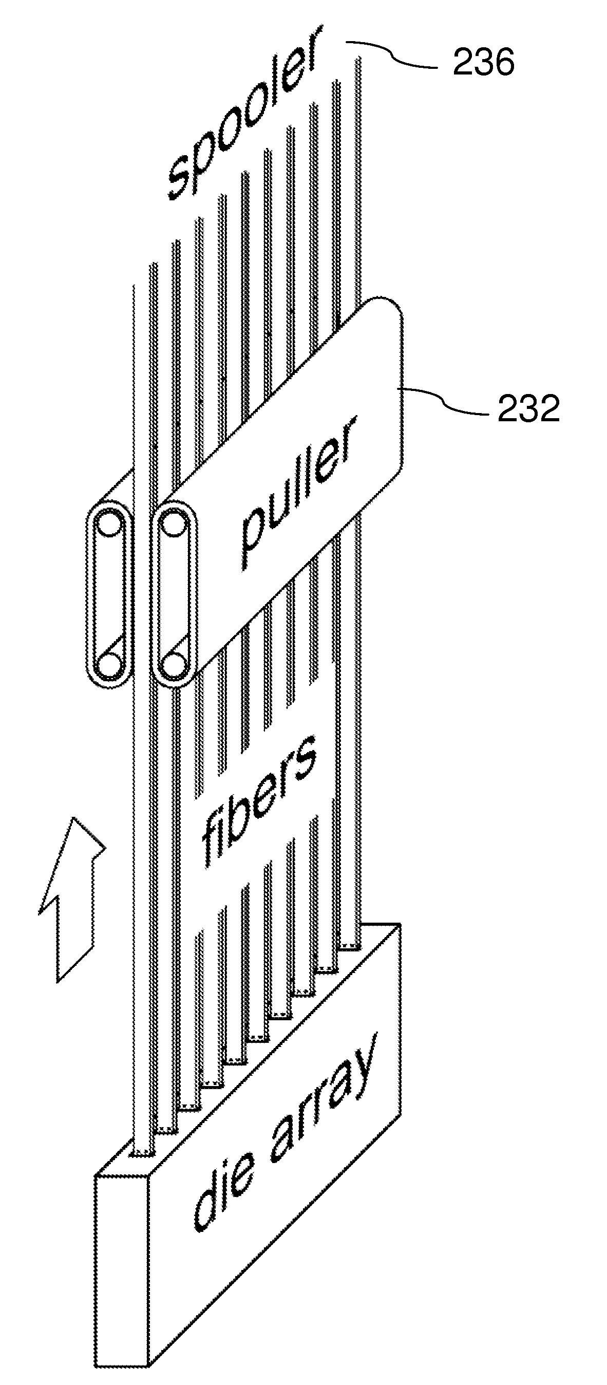
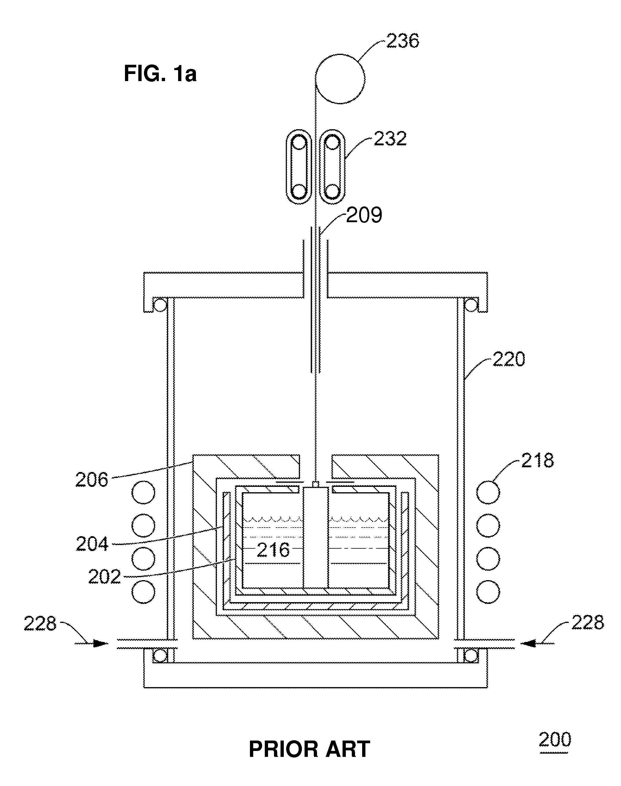
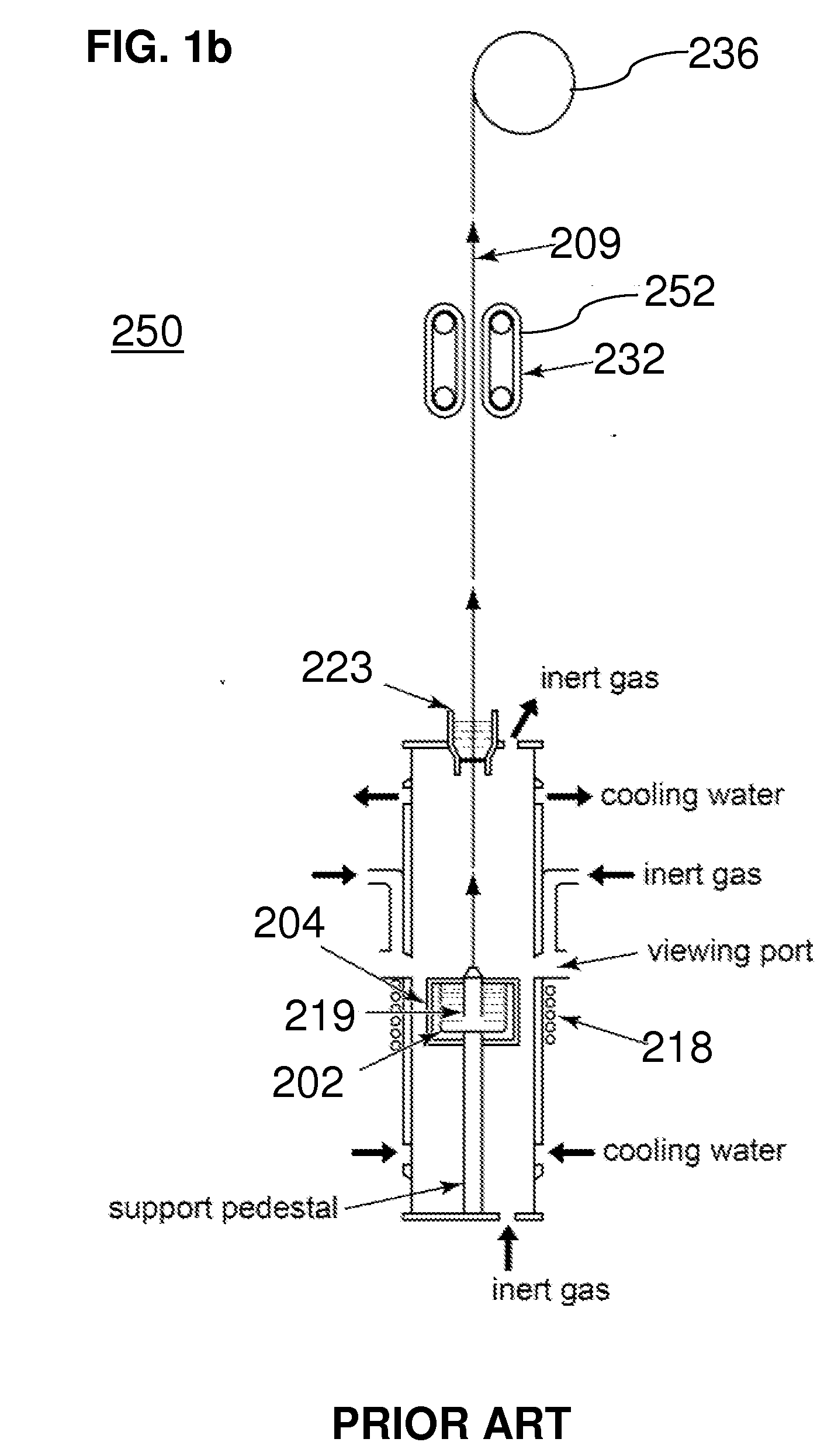
[0112]Using system 200 as shown FIG. 1, a structural sapphire fiber with R-plane facets according to the present invention was prepared. An initial sapphire seed of approximately ⅛″× 1 / 16″×1″ with a pointed end was attached to the die tip by melting the pointed end to the die tip. As noted above, it is known that the R planes of a sapphire crystal form a three-sided pyramid, with an 86° angle between the sides of the pyramid. The seed was cut so its axis lies along a corner of the pyramid. Thus, it has two R planes parallel to its axis. The R planes are at an angle of 86° to each other. One plane is coincident with the broad face of the seed. The seed was attached to a long, flat shaft, which can travel through the belt puller 232 shown in FIG. 1a. The puller was then placed as close to the tips as possible, and the initial fiber was drawn through the puller. The fiber resulting from this second operation is typically of good crystal orientation but can be of poor straightness. The ...

example 2

[0114]Again using system 200 described in FIG. 1a, a fiber of smaller dimensions was prepared. A fiber of cross-section 205 μm (thick)×460 μm (wide) was grown with two R-plane facets using a race-track shaped (composed of opposing semicircular end sections or curved edges and opposing straight parallel lines or flat faces) seed. The fiber was grown at a speed of 500 mm / hr, to a length of 848 mm. The sides of the racetrack-shaped fiber were flat. Table 2 gives the tilt of the R planes in the fiber. The “large face” is the broad, flat side of the fiber. The large face of the fiber is coincident to within 4.28° of an R plane. FIG. 24 shows a 2D detector image of the reciprocal lattice in relation to the fiber axis which is vertical was taken which revealed the R-planes being tilted by about 4° and 6° from the axis. FIG. 25 shows in schematic form the relationship of the R planes relative to the physical fiber in schematic form. An end view, a side view, and a front side view of the fib...

example 3

[0115]Using system shown in FIG. 1a, a sapphire fiber of was grown using a racetrack shaped seed containing two R-plane facets. The fiber grew stably to a length of approximately ten meters. Cross-section fracture mages of the fiber revealed that the fiber maintained its race-track shaped cross-section.

[0116]The above demonstrates that race-track shaped seeds can be used to create R-plane facets on a sapphire fiber. Racetrack-shaped fibers were found to grow robustly and stably, and have the potential to be extended to very long lengths without degradation of crystal structure. The crystal was oriented to give two pairs of R planes parallel to the growth axis. These R-plane facets can also result in miscut R-plane facets on the substrates, miscut by about 5 degrees. It is expected that the miscut of the facets will not have a detrimental effect on film growth especially with respect to superconductivity application and may in-fact be beneficial from a flux-pinning perspective (see e...


PUM

PropertyMeasurementUnit
lengthaaaaaaaaaa
speedaaaaaaaaaa
thickaaaaaaaaaa

Abstract

A crystalline article includes a single-crystal ceramic fiber, tape or ribbon. The fiber, tape or ribbon has at least one crystallographic facet along its length, which is generally at least one meter long. In the case of sapphire, the facets are R-plane, M-plane, C-plane or A-plane facets. Epitaxial articles, including superconducting articles, can be formed on the fiber, tape or ribbon.

Description

STATEMENT REGARDING FEDERALLY SPONSORED RESEARCH OR DEVELOPMENT[0001]The United States Government has rights in this invention pursuant to Contract No. DE-AC05-00OR22725 between the United States Department of Energy and UT-Battelle, LLC.FIELD OF THE INVENTION[0002]The present invention relates to the fabrication of faceted ceramic fibers, tapes or ribbons and epitaxial, functional layers thereon and / or devices prepared therefrom by deposition of one or more epitaxial layers on the surface of the facets.BACKGROUND OF THE INVENTION[0003]Many electrical, electronic, optical, magnetic, electromagnetic and electro-optical devices require single crystal-like device layers with few defects within the device layer for proper operation. For such applications, single-crystal or single-crystal-like devices offer the best performance. Fabrication of large-scale single-crystal-like devices can be accomplished by epitaxial growth of these devices on lattice-matched, single crystal substrates of ...

Claims


Application Information

Patent Timeline
Patent Type & Authority Applications(United States)
IPC IPC(8): C04B35/01B32B9/00C30B15/00H01L39/24
CPCC30B15/34Y10T428/2964C30B29/20C30B29/24C30B29/32C30B29/60C30B29/66H01L21/0242H01L21/02436H01L21/02521H01L39/2458H01L39/2461Y10S505/704Y10S505/701Y10T428/2973Y10T428/2958Y10T428/2924C30B29/16C30B29/64H10N60/0604H10N60/0632
Inventor GOYAL, AMIT
Owner UT BATTELLE LLC
Why Eureka
Try Eureka