Semiconductor device and method of processing the same

a semiconductor and device technology, applied in the direction of semiconductor devices, basic electric elements, electrical appliances, etc., can solve the problems of difficult to arrange multiple super junction structures in the wafer, and large number of processing steps

Active Publication Date: 2009-04-02
SEMICON COMPONENTS IND LLC
View PDF4 Cites 34 Cited by
  • Summary
  • Abstract
  • Description
  • Claims
  • Application Information

AI Technical Summary

Problems solved by technology

Thus, the conventional method has a problem that an extremely large number of processing steps are required.
Thus, there is a problem that a dep...

Method used


Image

  • Semiconductor device and method of processing the same
  • Semiconductor device and method of processing the same
  • Semiconductor device and method of processing the same

Examples


Embodiment Construction

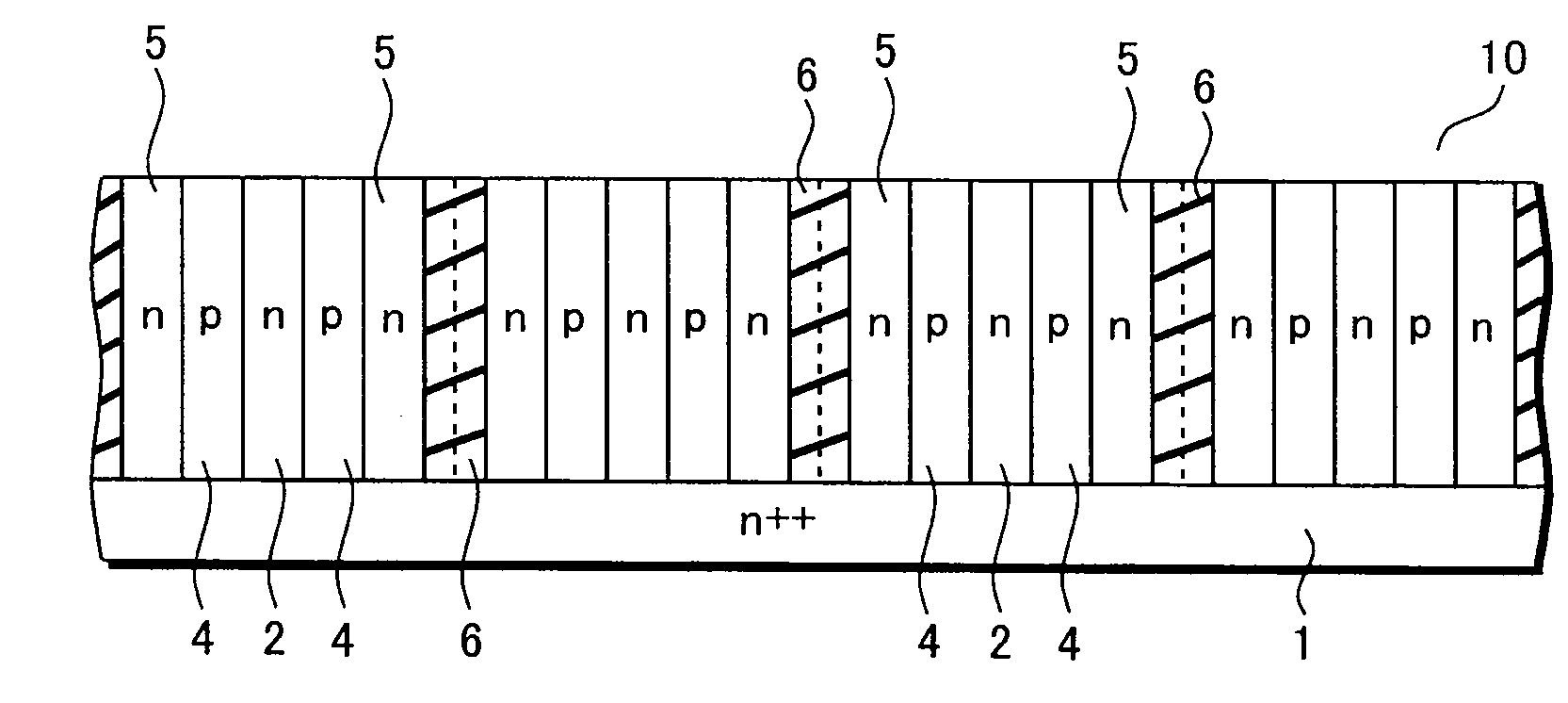
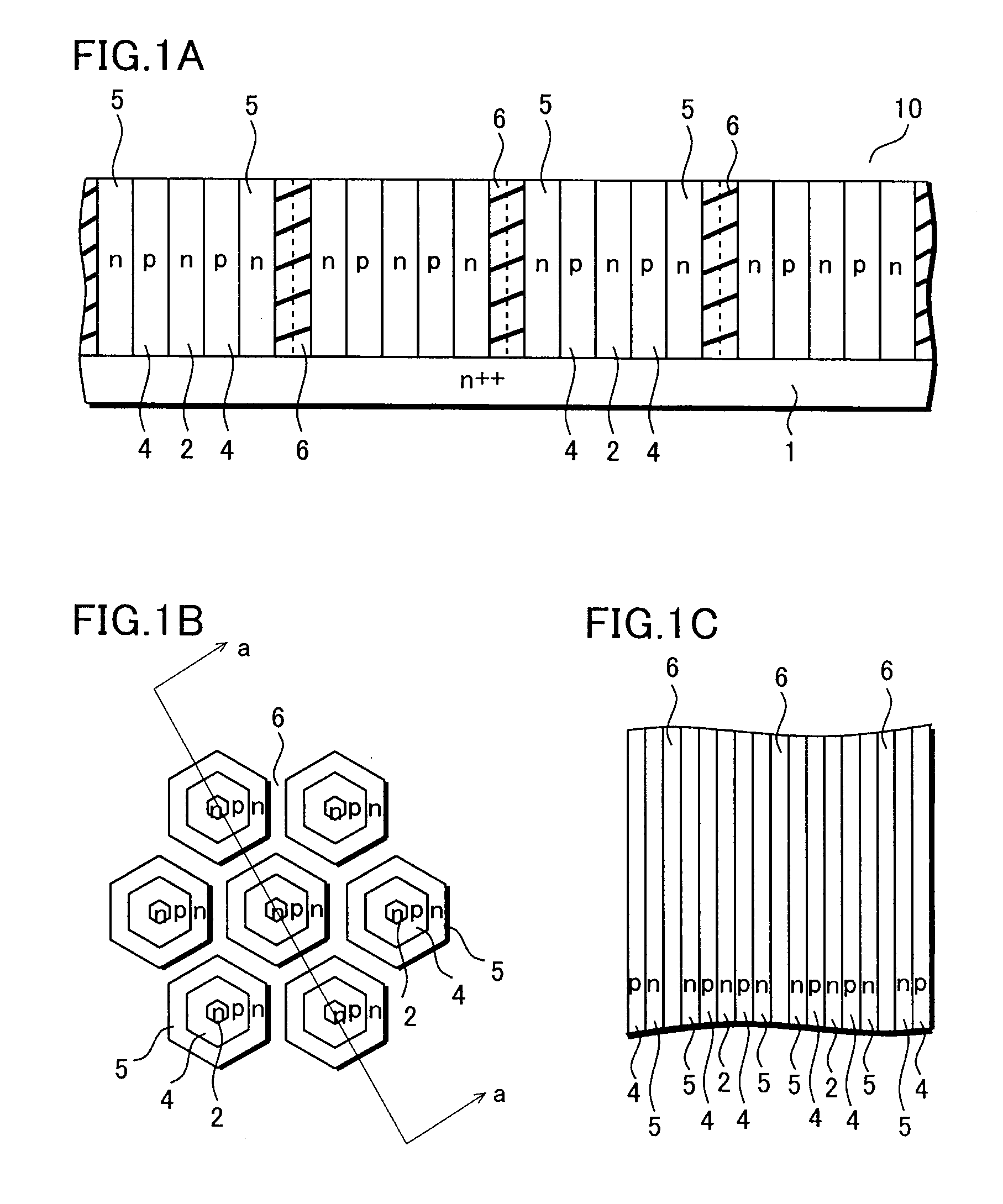
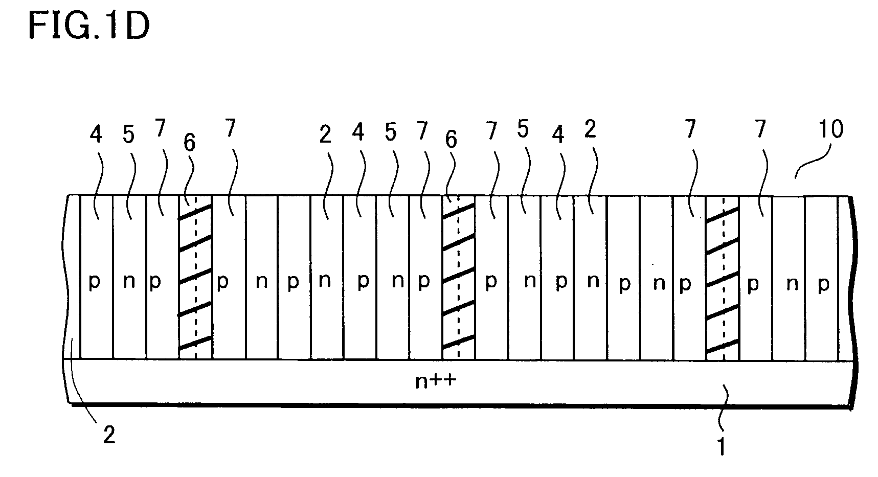
[0028]Embodiments of the present invention will be described below in detail by exemplarily taking a case where a semiconductor substrate is an n type silicon semiconductor substrate by referring to FIGS. 1A, 1B, 1C, 2, 3A, 3B, 4, 5, 6, 7, 8A, 8B, 9A and 9B.

[0029]A semiconductor wafer according to a preferred embodiment of the present invention includes one-conductivity-type semiconductor substrate, first to third semiconductor layers, and an insulating layer. In the semiconductor wafer, multiple pn junctions are provided in the vertical direction to a semiconductor wafer surface.

[0030]FIGS. 1A to 1C are views, each showing one example of a semiconductor wafer 10 according to the present embodiment. Specifically, FIG. 1A is a cross-sectional view, and FIGS. 1B and 1C are views, each showing a pattern of one principal surface of the semiconductor wafer 10. Note that, FIG. 1A is the cross-sectional view taken along the a-a line in FIG. 1B.

[0031]As shown in FIG. 1A, one-conductivity-ty...


PUM


Abstract

Provided is a semiconductor wafer. In the semiconductor wafer, formation and etching of an n type epitaxial layer and formation and etching of a p type epitaxial layer are alternately performed for at least three times, so that all semiconductor layers are formed of epitaxial layers on a semiconductor substrate. Thereby, the respective semiconductor layers can be formed to have reduced widths. Thus, if a required breakdown voltage is the same, dopant concentrations of the respective semiconductor layers can be increased and a resistance value of the wafer can be reduced. In addition, a space portion remaining in the end is buried with an insulating layer, so that a defect can be avoided in a junction surface of the epitaxial layers.

Description

[0001]This application claims priority from Japanese Patent Application Number JP 2007-252200 filed on Sep. 27, 2007, the content of which is incorporated herein by reference in its entirety.BACKGROUND OF THE INVENTION[0002]1. Field of the Invention[0003]The present invention relates to a method for processing a semiconductor wafer. In particular, the present invention relates to shortening a process of processing a semiconductor wafer achieving high breakdown voltage and low on-resistance and to a method for processing a semiconductor wafer with improved characteristics.[0004]2. Description of the Related Art[0005]As a silicon semiconductor wafer achieving high breakdown voltage and low on-resistance, known is a wafer structure in which pillar-like p type semiconductor regions and n type semiconductor regions are provided so as to form multiple pn junctions vertical to a wafer surface. This technology is described for instance in International Patent Publication No. WO02 / 067333, Pa...

Claims


Application Information

Patent Timeline
IPC IPC(8): H01L27/00H01L21/20
CPCH01L21/02381H01L21/0243H01L21/02439H01L21/02494H01L21/02521H01L21/02573H01L21/8222H01L21/02656H01L21/761H01L21/76224H01L21/764H01L21/82H01L21/02587
Inventor ISHIDA, HIROYASUSAYAMA, YASUYUKI
Owner SEMICON COMPONENTS IND LLC
Why Eureka
Try Eureka