

Vertical diode based memory cells having a lowered programming voltage and methods of forming the same
- Summary
- Abstract
- Description
- Claims
- Application Information
AI Technical Summary
Problems solved by technology
Method used
Image

Examples
Embodiment Construction
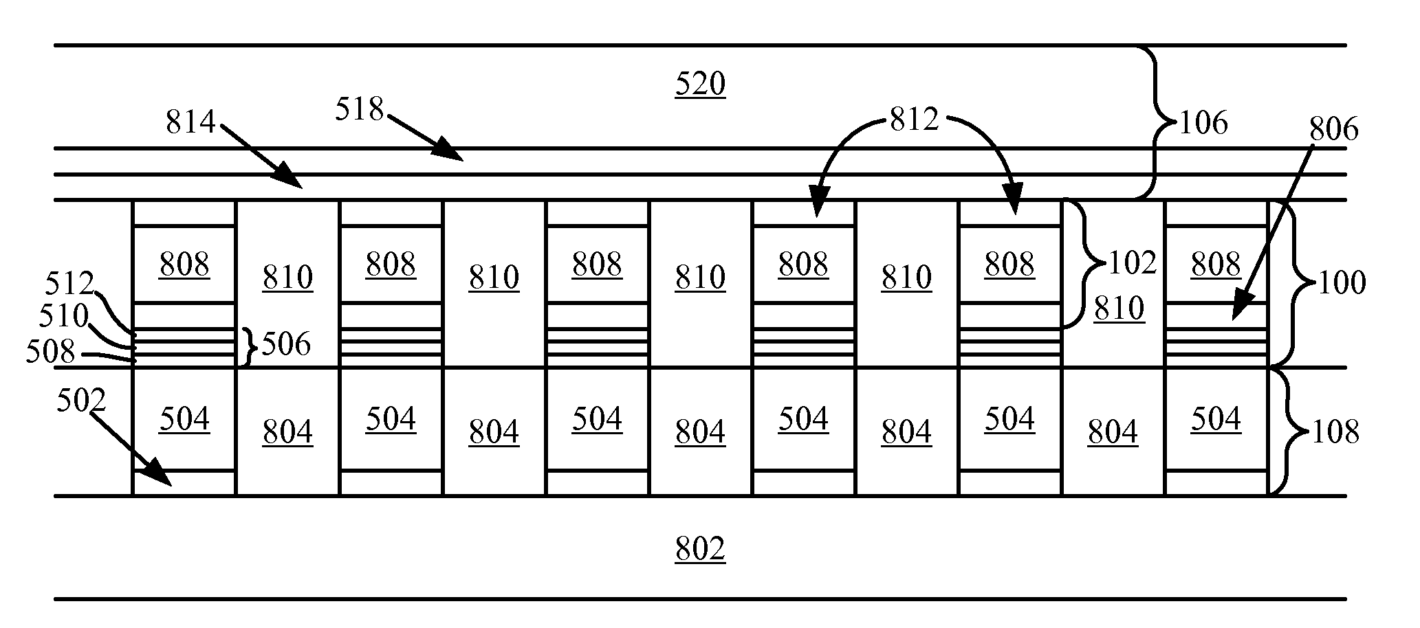
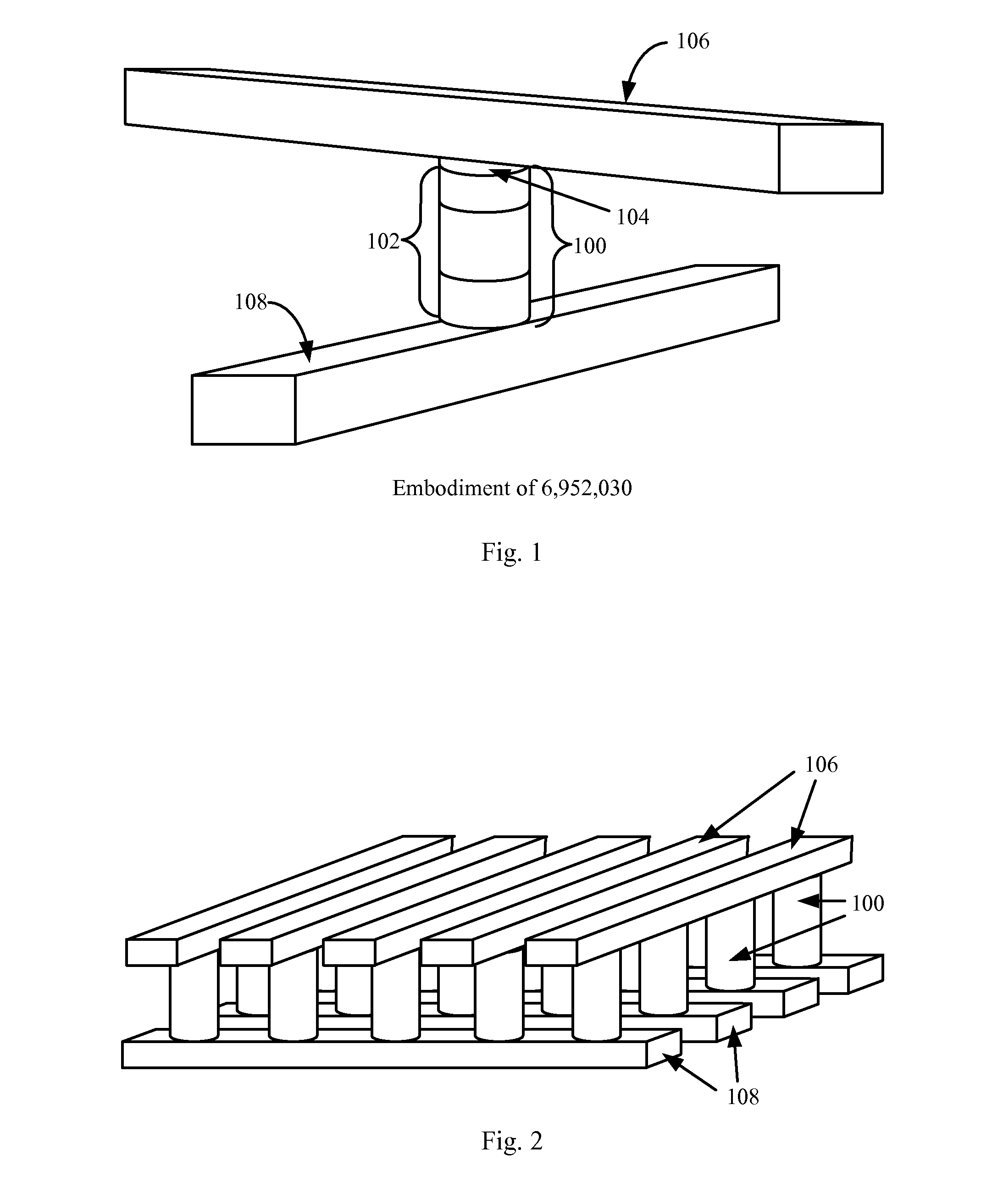
[0020]FIG. 1 shows an embodiment of a memory cell described in Herner et al., U.S. Pat. No. 6,952,030, “High-density three-dimensional memory cell,” hereinafter the '030 patent. In this nonvolatile memory cell, pillar 100 includes a diode 102 and a dielectric rupture antifuse 104 arranged electrically in series between top conductor 106 and bottom conductor 108. In the initial state of this memory cell, when a read voltage is applied between top conductor 106 and bottom conductor 108 very little current flows between them. Application of a relatively large programming voltage permanently alters the memory cell of FIG. 1 so that, after programming, much more current flows at the same read voltage. This difference in current under the same applied read voltage allows a programmed cell to be distinguished from an unprogrammed cell; for example for a data “0” to be distinguished from a data “1”.
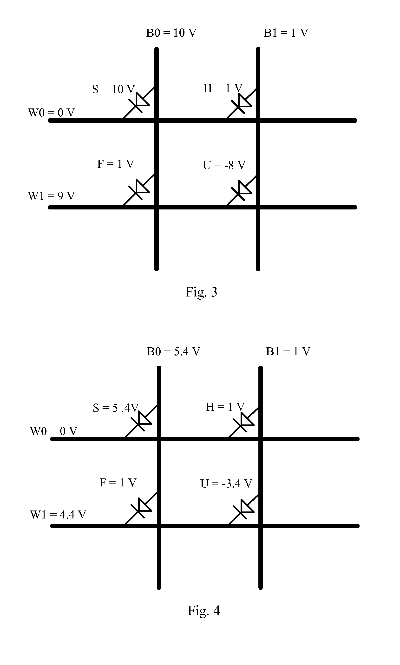
[0021]As described in detail in Herner et al., U.S. patent application Ser. No. 10 / 955,549, “...
PUM
 Abstract
Description
Claims
Application Information