
Light emitting module and method for manufacturing the same

a technology of light-emitting modules and manufacturing methods, which is applied in the manufacture of printed circuits, printed circuit aspects, metal core circuits, etc., can solve the problems of large heat dissipation, poor heat dissipation effect, and the inability to desirably dissipate heat from the led to the outside, and achieves high heat dissipation properties

Inactive Publication Date: 2009-04-09
SANYO ELECTRIC CO LTD +2
View PDF3 Cites 39 Cited by
  • Summary
  • Abstract
  • Description
  • Claims
  • Application Information

AI Technical Summary

Benefits of technology

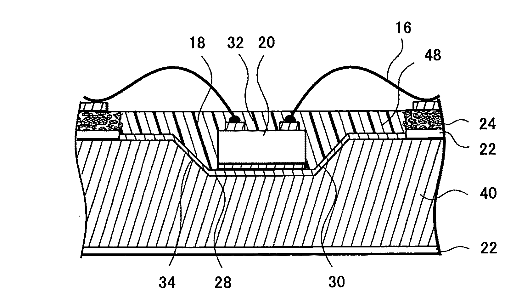
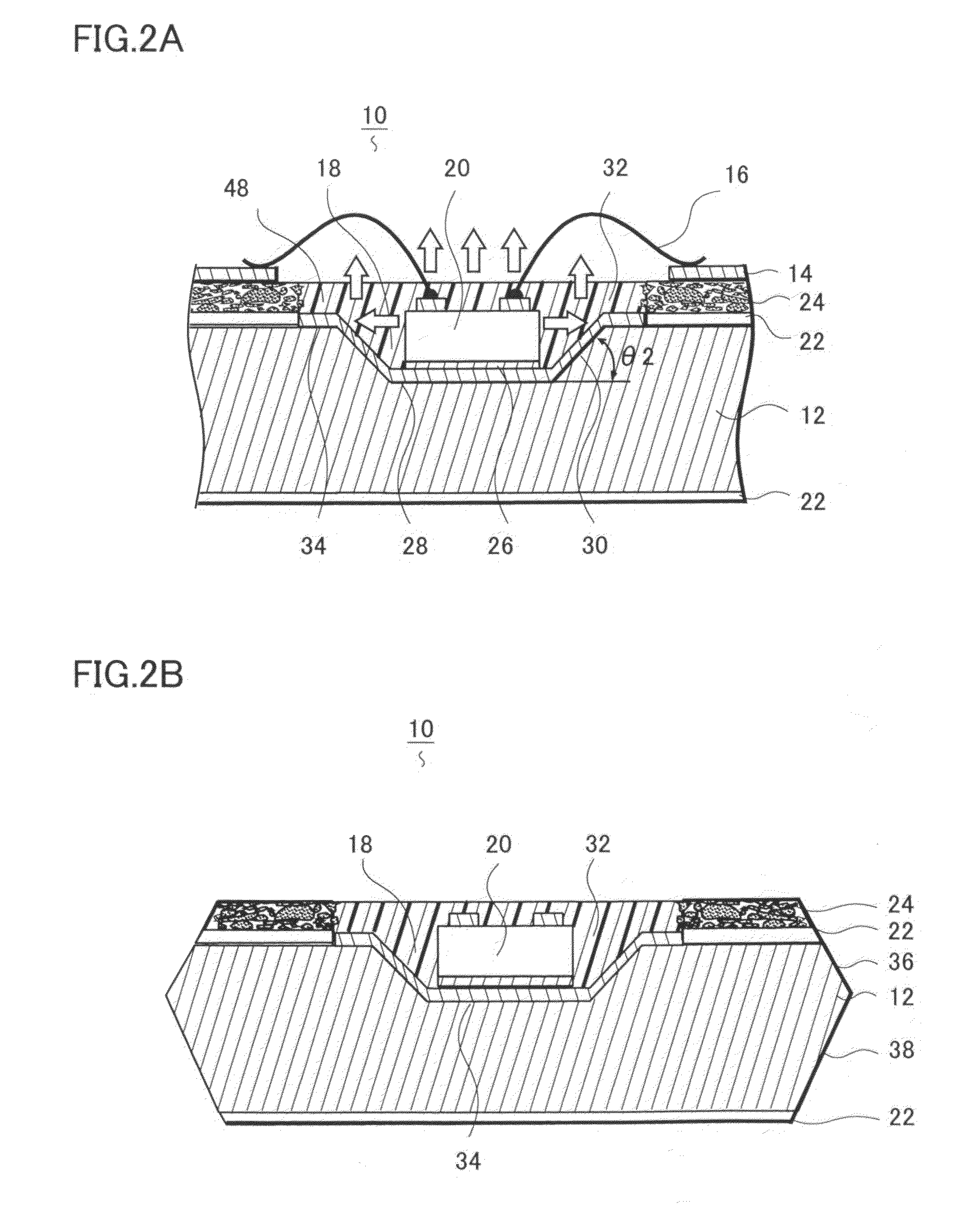
[0013]A light emitting module according to the present invention includes: a metal substrate whose first main surface is covered with an insulating layer; a conductive pattern formed on a main surface of the insulating layer; and a light emitting element electrically connected to the conductive pattern. A groove is formed in the metal substrate in a second main surface of the metal substrate, and at a position where the groove is formed, the metal substrate is bent to a side opposite to a side where the light emitting element is mounted.
[0014]A method for manufacturing a light emitting module according to the present invention includes the steps of: forming a conductive pattern on a main surface of an insulating layer covering a first main surface of a metal substrate; forming a groove in a second main surface of the metal substrate; fixedly attaching a light emitting element on the first main surface of the metal substrate, and electrically connecting the light emitting element to the conductive pattern; and at a position where the groove is formed, bending the metal substrate to a side opposite to a side where the light emitting element is mounted.
[0014]A method for manufacturing a light emitting module according to the present invention includes the steps of: forming a conductive pattern on a main surface of an insulating layer covering a first main surface of a metal substrate; forming a groove in a second main surface of the metal substrate; fixedly attaching a light emitting element on the first main surface of the metal substrate, and electrically connecting the light emitting element to the conductive pattern; and at a position where the groove is formed, bending the metal substrate to a side opposite to a side where the light emitting element is mounted.

Problems solved by technology

When used in lighting equipment, a large number of LEDs are mounted in single lighting equipment, because merely a single LED cannot produce sufficient brightness.
However, an LED dissipates a large amount of heat during the light emission.
Accordingly, when an LED is mounted on a mounting board made of a resin material that has an inferior heat-dissipating property, or when such LEDs are resin-packaged individually, heat is not desirably dissipated from the LED to the outside.
Consequently, the performance of the LED is deteriorated soon.
Nevertheless, the technology described in Patent Document 1 aims to incorporate only one packaged LED in the light source unit, and thus is not made on the assumption that multiple LEDs are mounted in a light source unit.
Accordingly, the light source unit described in this document produces an insufficient amount of light for use for illumination or the like.
Thus, unless the heat from the LEDs is desirably dissipated, the temperature of the entire unit may increase so high that the heat will decrease the conversion efficiency of LEDs, or destroy the LEDs.
Accordingly, it has been difficult to incorporate the metal substrate 11 having an LED mounted thereon, for example, inside a set having a complicated shape (such as a corner of an automobile or the interior of a toy).

Method used


Image

  • Light emitting module and method for manufacturing the same
  • Light emitting module and method for manufacturing the same
  • Light emitting module and method for manufacturing the same

Examples


first embodiment

Configuration of Light Emitting Module

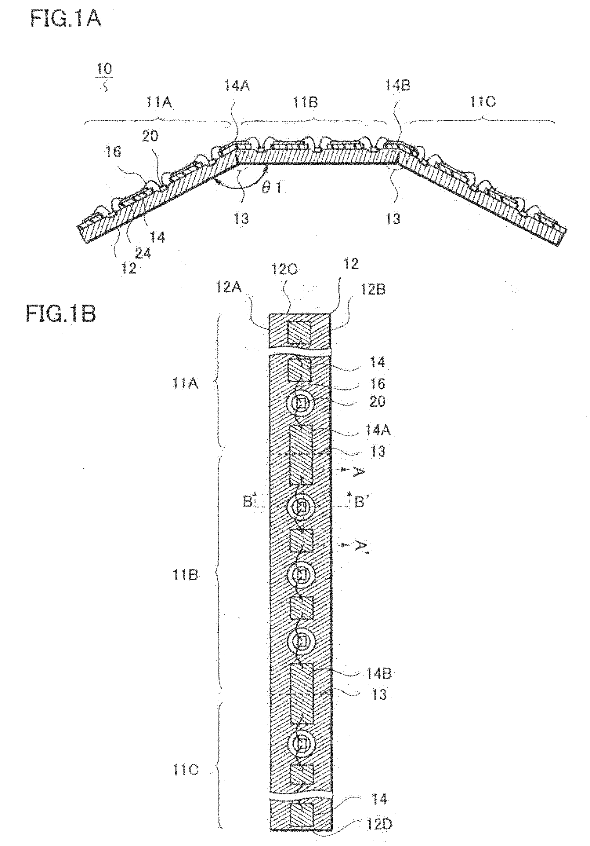
[0030]In this embodiment, a configuration of a light emitting module 10 will be described with reference to FIG. 1A to FIG. 3B.

[0031]FIG. 1A is a cross-sectional view of the light emitting module 10. FIG. 1B is a plan view of the light emitting module 10 seen from top.

[0032]As shown in FIG. 1A, the light emitting module 10 mainly includes: a metal substrate 12; an insulating layer 24 covering the upper surface of the metal substrate 12; a conductive pattern 14 formed on the upper surface of the insulating layer 24; and a light emitting element 20 fixedly attached to the upper surface of the metal substrate 12 and electrically connected to the conductive pattern 14.

[0033]The light emitting module 10 has the multiple light emitting elements 20 mounted on the upper surface of the single plate-like metal substrate 12. These light emitting elements 20 are connected to each other in series via the conductive patterns 14 and thin metal wires 16. By sup...

second embodiment

Method for Manufacturing Light Emitting Module

[0074]Hereinafter, a method for manufacturing a light emitting module 10 with the above-described configuration will be described with reference to FIG. 4A to FIG. 13B.

[0075]First step: see FIGS. 4A to 4C

[0076]As shown in FIGS. 4A to 4C, firstly, a substrate 40 that is a base member for the light emitting module 10 is prepared, and a conductive pattern is formed.

[0077]Refer to FIG. 4A. At first, the substrate 40 is made of a metal that has, for example, copper or aluminium as the main material, and has a thickness of approximately 0.5 mm to 2.0 mm. The planar size of the substrate 40 is, for example, approximately 1 m×1 m, and the single substrate 40 produces multiple light emitting modules. When the substrate 40 is a substrate made of aluminium, the upper surface and the lower surface of the substrate 40 are covered with the above-described anodized film.

[0078]The upper surface of the substrate 40 is entirely covered with an insulating ...

third embodiment

Description of Experimental Results

[0122]In this embodiment, with reference to FIGS. 14A to 14E, description will be given of experimental results by which the influence of metal-substrate bending on a conductive pattern is confirmed. FIG. 14A is a photograph of a bent metal substrate, taken from a side of the metal substrate. FIGS. 14B, 14C, 14D and 14E are Scanning Electron Microscope (SEM) images obtained by taking a photo of conductive patterns at bent portions after metal substrates are bent, while the metal substrates are heated at various temperatures.

[0123]As shown in FIG. 14A, a metal substrate is bent according to the method described in the second embodiment. The upper surface of the metal substrate is covered with an insulating layer made of a polyimide insulating resin. A conductive pattern is formed on the upper surface of this insulating layer. Here, an angle θ4 formed by bending the metal substrate is 148° in the actual measurement.

[0124]FIG. 14B is an SEM image obta...


PUM


Abstract

Provided are: a light emitting module capable of ensuring a high heat-dissipating property and mountable in any of sets in various shapes; and a method for manufacturing the light emitting module. The light emitting module mainly includes: a metal substrate; an insulating layer covering the upper surface of the metal substrate; a conductive pattern formed on the upper surface of the insulating layer; and a light emitting element fixedly attached to the upper surface of the metal substrate and electrically connected to the conductive pattern. Furthermore, a groove is formed in the metal substrate, and then the metal substrate is bent. Thus, a bent portion is formed in the metal substrate.

Description

[0001]This application claims priority from Japanese Patent Application Number JP 2007-247875 filed on Sep. 25, 2007, the content of which is incorporated herein by reference in its entirety.BACKGROUND OF THE INVENTION[0002]1. Field of the Invention[0003]The present invention relates to a light emitting module and a method for manufacturing the same. Particularly, the present invention relates to a light emitting module on which a high-luminance light emitting element is mounted, and a method for manufacturing the light emitting module.[0004]2. Description of the Related Art[0005]A semiconductor light emitting element represented by a light emitting diode (LED) has a long life and shows a high visibility. Accordingly, its use in traffic signals, lamps of automobiles, and the like, has been started. Moreover, use of an LED in lighting equipment is emerging.[0006]When used in lighting equipment, a large number of LEDs are mounted in single lighting equipment, because merely a single L...

Claims


Application Information

Patent Timeline
Patent Type & Authority Applications(United States)
IPC IPC(8): H01L33/00H01L33/32H01L33/60H01L33/64
CPCH01L25/0753H01L33/483H01L2924/07802H01L2224/73265H01L2224/48465H01L2224/48091H01L24/97H01L2224/48227H01L2924/12041H05K2203/302H05K2203/0315H05K1/0203H05K1/021H05K1/056H05K1/182H05K1/189H05K3/0014H05K3/0052H05K3/44H05K2201/09745H05K2201/10106H01L2924/00014H01L2924/00
Inventor MORI, HARUHIKOKUSABE, TAKAYAMOTOIKE, TATSUYA
Owner SANYO ELECTRIC CO LTD
Learn More