Touch-sensing display device and method for manufacturing the same

a display device and touch sensor technology, applied in semiconductor devices, instruments, computing, etc., can solve the problems of reducing transmittance, difficult to produce a light and slim touch panel display device, and too much weight and total thickness of the device, and achieve the effect of high transparency and low cos

Active Publication Date: 2009-04-16
AU OPTRONICS CORP
View PDF3 Cites 28 Cited by
  • Summary
  • Abstract
  • Description
  • Claims
  • Application Information

AI Technical Summary

Benefits of technology

[0032]Hence, the display device of the present invention, which has a touch-sensing element integrated in (or assembled with) the first substrate, can be

Problems solved by technology

However, in such device having a touch screen on one surface of the display panel, the total weight and total thickness thereof are too great, and is difficult to produce a light and slim touch panel display devic

Method used


Image

  • Touch-sensing display device and method for manufacturing the same
  • Touch-sensing display device and method for manufacturing the same
  • Touch-sensing display device and method for manufacturing the same

Examples


example 1

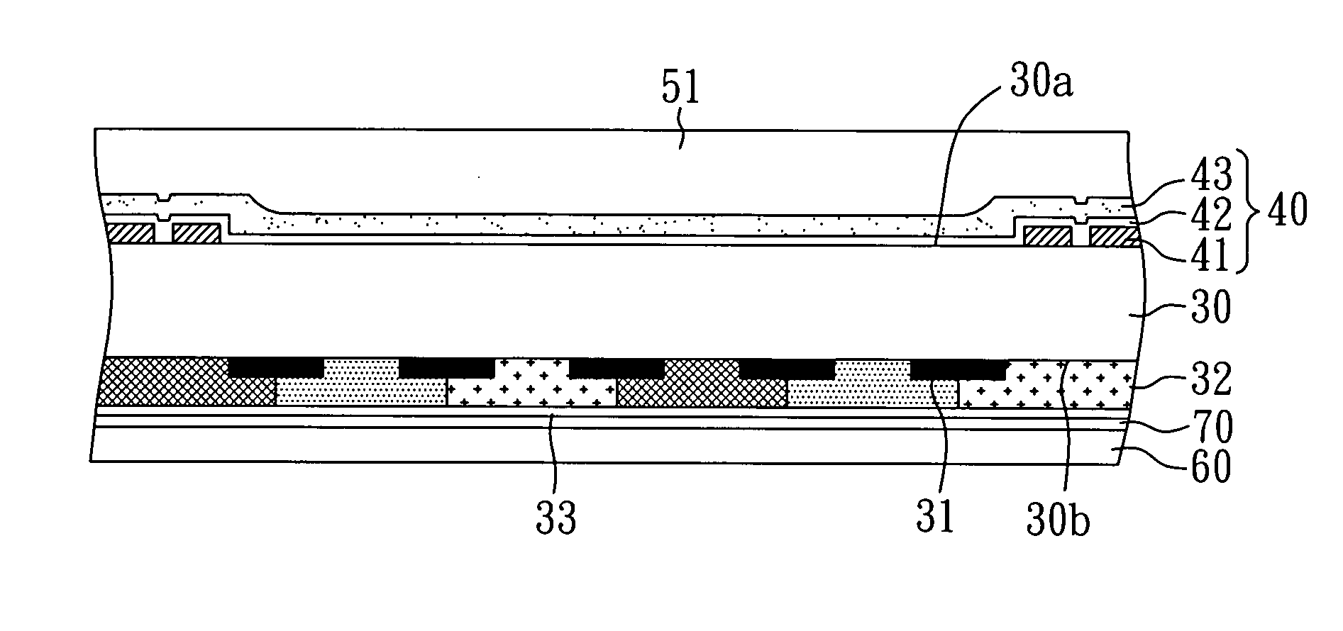
[0045]Referring to both FIGS. 2 and 3, wherein a schematic view of a display device and a process flow chart of the first substrate are shown respectively, the method of providing a display device of the present example is described below.

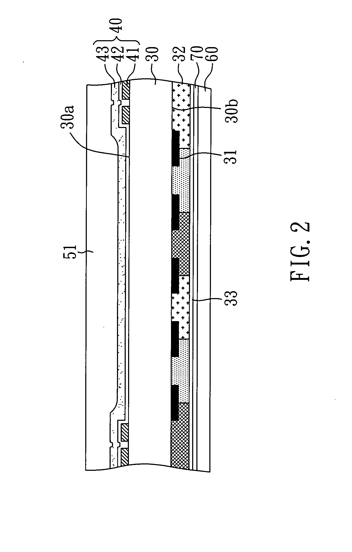
[0046]First, a first substrate 30 having a first surface 30a and a second surface 30b is provided. Herein, the first substrate 30 can be a glass substrate.

[0047]Then, a touch-sensing element 40 is formed on the first surface 30a of the first substrate 30, wherein the steps of forming the touch-sensing element 40 comprise: forming a patterned electrode 41 on the first surface 30a of the first substrate 30, in which the electrode layer 41 may be made of molybdenum / aluminum (Mo / Al) (Al formed before the formation of Mo) or Mo / Al / Mo (Mo formed first, following with Al, and then Mo formed at last). Herein, the patterned electrode 41 locates correspondingly on the periphery of the first substrate 30, as shown in FIG. 4. However, the tracing line and the ...

example 2

[0051]This is the same method as in Example 1, except that a polarizing material or a polarizing element, which is able to polarize lights, is directly used to replace the silicon nitride (SiNx) to form the passivation layer 431 on the conductive layer 42 and on the patterned electrode 41 of the present example (as shown in FIG. 6). Thereby, the passivation layer 431 of the present example is able to possess the polarizing function (the same as that of the polarizing element 51, as shown in FIG. 2) and passivation function at the same time. Hence, there is no excess need of attaching the polarizing element 51 (as shown in FIG. 2). Other steps are the same as those of Example 1 to produce a display device.

example 3

[0052]With reference to FIGS. 7 and 8, the method of fabricating a display device here is the same as that of Example 1, except that the conductive layer 42 is firstly formed on the first surface 30a of the first substrate 30, then the formation of the patterned electrode 41 electrically connected to the conductive layer 42 follows when producing the touch-sensing element 40. The electrode layer 41 may be made of Al / Mo (Al formed after the formation of Mo) or Mo / Al / Mo (Mo formed first, following with Al, and then Mo formed at last). The patterned electrode 41 locates correspondingly on the periphery of the first substrate 30, and the layout of the patterned electrode 41 may be the same as that in Example 1. Other steps are the same as those of Example 1 to produce a display device.


PUM


Abstract

A display device and method for manufacturing the same are disclosed. The display device includes a first substrate, a second substrate, a touch-sensing element, and a liquid crystal. The first substrate has a first surface and a second surface thereon. The second substrate has a pixel array and is disposed on the second surface of the first substrate. The touch-sensing element locates on the first surface of the first substrate. Furthermore, the touch-sensing element includes a conductive layer, a patterned electrode, and a passivation layer. The patterned electrode is correspondingly located on the periphery of the first substrate, and electrically connected to the conductive layer. The passivation layer covers the conductive layer and the patterned electrode. In addition, the liquid crystal is disposed between the first substrate and the second substrate.

Description

BACKGROUND OF THE INVENTION[0001]1. Field of the Invention[0002]The present invention relates to a touch panel display device, and more particularly relates to a light and slim touch panel display device.[0003]2. Description of Related Art[0004]Touch panel display devices, in which the information data is input by touching with fingers or styli on the display area, are extensively used in personal computers, notebooks, personal digital assistants (PDAs), or other similar devices.[0005]A conventional touch panel display device comprises a display panel and a touch screen attached to the display panel. The touch screen can include at least four technologies, including: capacitive, resistive, surface acoustic wave (SAW), and infrared (optical). As for the general touch screens located in public applications, a capacitive touch screen is often used. With reference to FIG. 1, a conventional touch panel display device is represented, wherein a touch panel display device comprises: a displ...

Claims


Application Information

Patent Timeline
IPC IPC(8): H01L33/00G06F3/042
CPCG06F3/044G06F3/0412G06F3/0443
Inventor LIU, PO-YUANLAI, MING-SHENGLIU, CHUN-HSINTSAI, KUN-HUA
Owner AU OPTRONICS CORP
Why Eureka
Try Eureka