Coater/developer, method of coating and developing resist film, and computer readable storing medium

a technology of resist film and coating, applied in the direction of liquid surface applicators, coatings, pretreated surfaces, etc., can solve the problems of increased running cost, increased fabrication cost, and inability to use modules mounted in the coater/developer, so as to reduce the running cost

Active Publication Date: 2009-04-16
TOKYO ELECTRON LTD
View PDF3 Cites 34 Cited by
  • Summary
  • Abstract
  • Description
  • Claims
  • Application Information

AI Technical Summary

Benefits of technology

[0025]According to an embodiment of the present invention waste of electricity and running cost can be reduced because the number of modules to be used can be automatically determined in a coater / developer.

Problems solved by technology

However, all the modules mounted in the coater / developer are not used in every process.
What is worse in this situation is that all the nine heating modules start to be heated to 90° C. through 130° C. when selected by the operator, which leads to a waste of electricity, an increased running cost and thus an increased fabrication cost.
Patent-related Document 1 fails to disclose or suggest a way of reducing the waste of electricity and the running cost.

Method used


Image

  • Coater/developer, method of coating and developing resist film, and computer readable storing medium
  • Coater/developer, method of coating and developing resist film, and computer readable storing medium
  • Coater/developer, method of coating and developing resist film, and computer readable storing medium

Examples


Embodiment Construction

[0041]Non-limiting, exemplary embodiments of the present invention will now be described with reference to the accompanying drawings. In the drawings, the same or corresponding reference marks are given to the same or corresponding members or components and hence repetitive explanations are omitted. It is to be noted that the drawings are illustrative of the invention, and there is no intention to indicate scale or relative proportions among the members or components. Therefore, the specific size should be determined by a person having ordinary skill in the art in view of the following non-limiting embodiments.

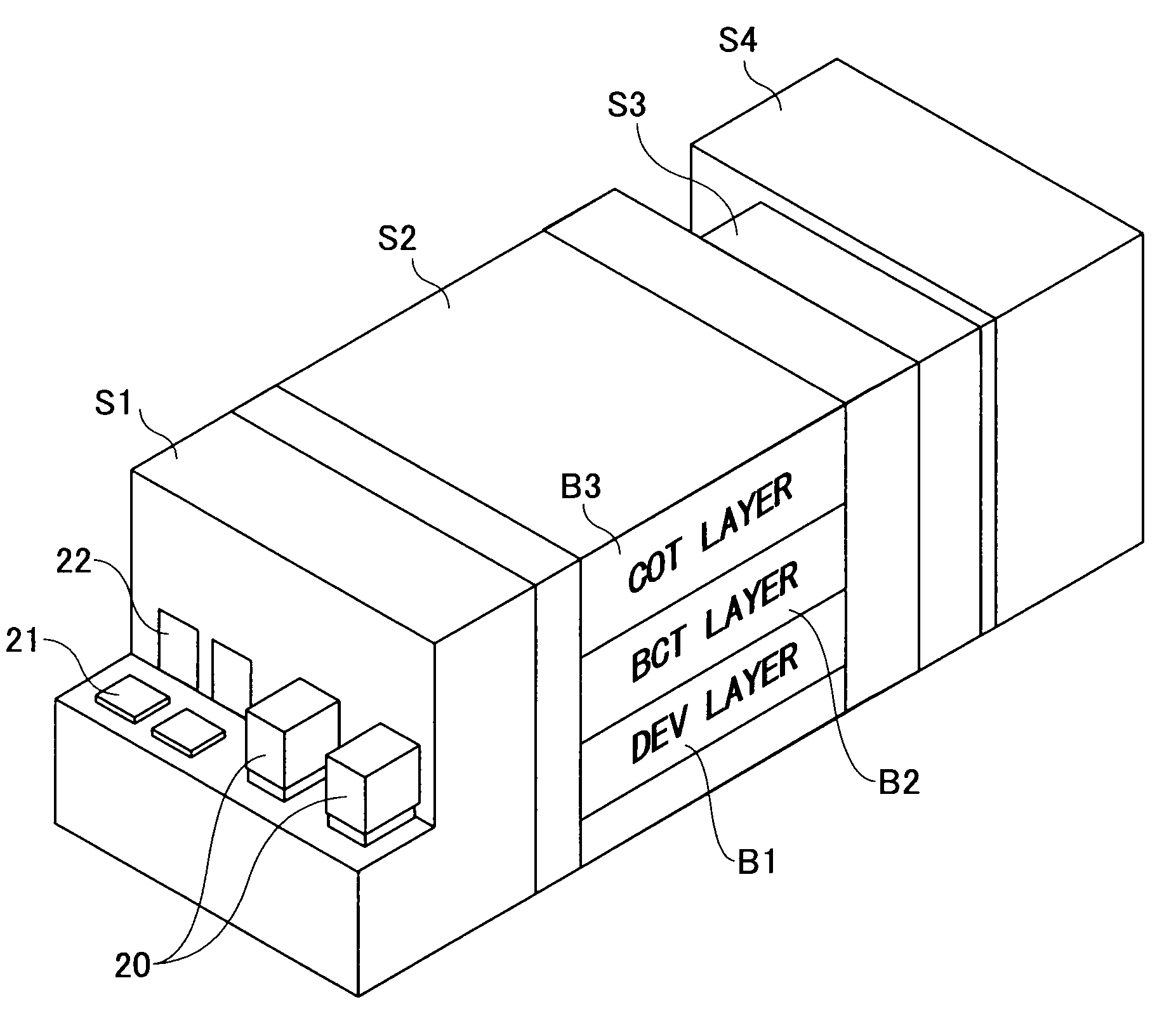
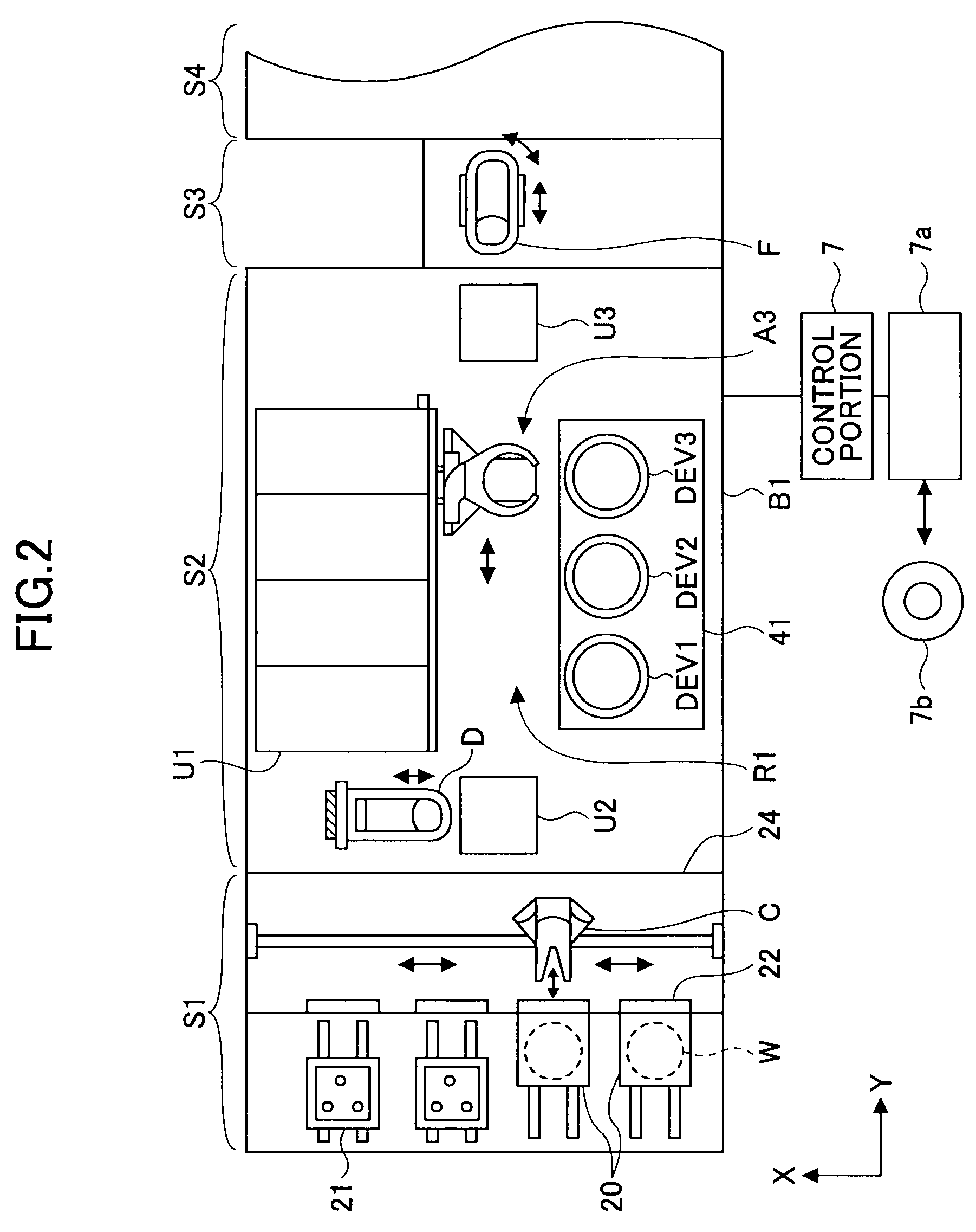
[0042]Referring to the accompanying drawings, a resist pattern forming apparatus including a coater / developer according to an embodiment of the present invention is described. FIG. 2 is a plan view of the resist pattern forming apparatus. FIG. 3 is a perspective view of the resist pattern forming apparatus of FIG. 2. FIG. 4 is a side view of the resist pattern forming apparatu...


PUM


Abstract

A transfer flow is produced in accordance with a process recipe of a process to be carried out. In the transfer flow, a type of modules listed in accordance with a substrate transfer order is associated with a necessary staying time from when the substrate is transferred into a module by a substrate transfer unit to when the substrate is ready to be transferred back to the substrate transfer unit after the corresponding process is finished. A cycle limiting time is determined to be the longest necessary transfer cycle time among those obtained by dividing the necessary staying time by the number of the modules mounted in the coater/developer. The number of the modules to be used is determined to be a value obtained by dividing the necessary staying time by the cycle limiting time or a nearest integer to which the value is raised.

Description

BACKGROUND OF THE INVENTION[0001]1. Field of the Invention[0002]The present invention relates to a coater / developer that coats a resist film on a substrate such as a semiconductor wafer, an LCD wafer (glass wafer for an Liquid Crystal Display) and develops the exposed resist film, a method of coating and developing the resist film, and a computer readable storing medium that stores a program for allowing the coater / developer to carry out the method of coating and developing the resist film.[0003]2. Description of the Related Art[0004]In a fabrication process of a semiconductor device or a flat panel display (FPD), photolithography is indispensable in order to form a predetermined resist pattern on a substrate. The photolithography includes a series of processes of coating resist solution in order to form a resist film on the substrate such as a semiconductor wafer (referred to as a wafer below), exposing the resist film with exposure light through a photomask, and developing the res...

Claims


Application Information

Patent Timeline
Patent Type & Authority Applications(United States)
IPC IPC(8): B05D3/02B05C11/02
CPCH01L21/67276
Inventor MIYATA, AKIRATATEYAMA, MASANORI
Owner TOKYO ELECTRON LTD
Why Eureka
Try Eureka