

Object cutting method
a cutting method and object technology, applied in the field of object cutting method, can solve the problem that the modified region is difficult to remove the remaining particles of the cut section of the chip, and achieve the effect of preventing the modification
- Summary
- Abstract
- Description
- Claims
- Application Information
AI Technical Summary
Benefits of technology
Problems solved by technology
Method used
Image

Examples
first embodiment
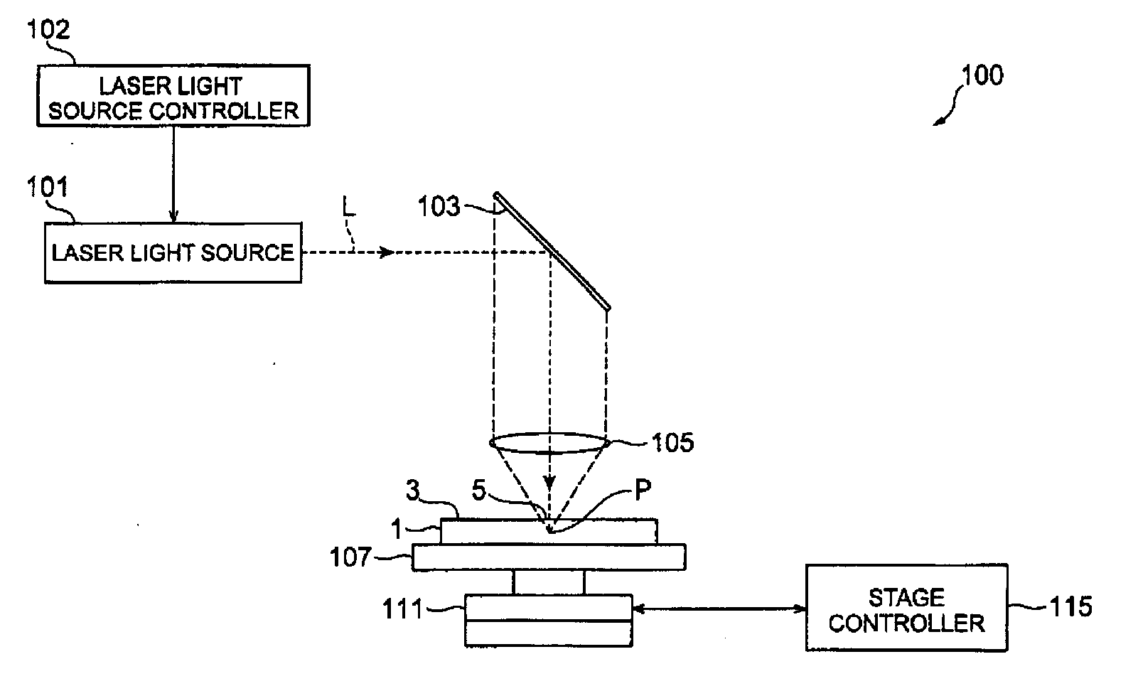
[0076]FIG. 10 is a plan view of an object to be processed for which the object cutting method in accordance with the first embodiment is employed, while FIG. 11 is a sectional view of a part of the object of FIG. 10 taken along a line to cut. As shown in FIGS. 10 and 11, a planar object to be processed 1 comprises a silicon wafer (semiconductor substrate) 11 and a functional device layer 16, formed on a main face of the silicon wafer 11, including a plurality of functional devices 15. A number of functional devices 15, examples of which include semiconductor operating layers formed by crystal growth, light-receiving devices such as photodiodes, light-emitting devices such as laser diodes, and circuit devices formed as circuits, are formed like a matrix in directions parallel and perpendicular to an orientation flat 6 of the silicon wafer 11 in the first embodiment.
[0077]The object cutting method in accordance with the first embodiment is employed for the object 1 constructed as ment...
second embodiment
[0090]The second embodiment is the same as the first embodiment up to the step of constructing the semiconductor chip supporting unit 26.
[0091]After being constructed, the semiconductor chip supporting unit 26 is supported such that the expandable tape 23 faces up (i.e., the semiconductor chips 25 and expandable tape 23 are positioned such that the expandable tape 23 is located higher than the semiconductor chips 25 in the vertical direction) as shown in FIG. 16(a), and the adsorption tape (second sheet) 27 is arranged such as to oppose the expandable tape 23 while holding the semiconductor chips 25 therebetween. Then, as shown in FIG. 16(b), an ion generator 54 generates a chargeable ion flow (second ion flow; e.g., an ion flow including a positive or negative ion), so that the adsorption tape 27 is irradiated therewith from the lower side and electrically charged.
[0092]Subsequently, as shown in FIG. 17, the ion generator 53 generates a chargeable ion flow (first ion flow; e.g., an...
third embodiment
[0096]In the third embodiment, the object to be processed 1 is a so-called MEMS wafer. A number of functional devices 15, examples of which include mechanical element members, sensors, actuators, and electronic circuits, are formed like a matrix in directions parallel and perpendicular to the orientation flat 6 of the silicon wafer 11.
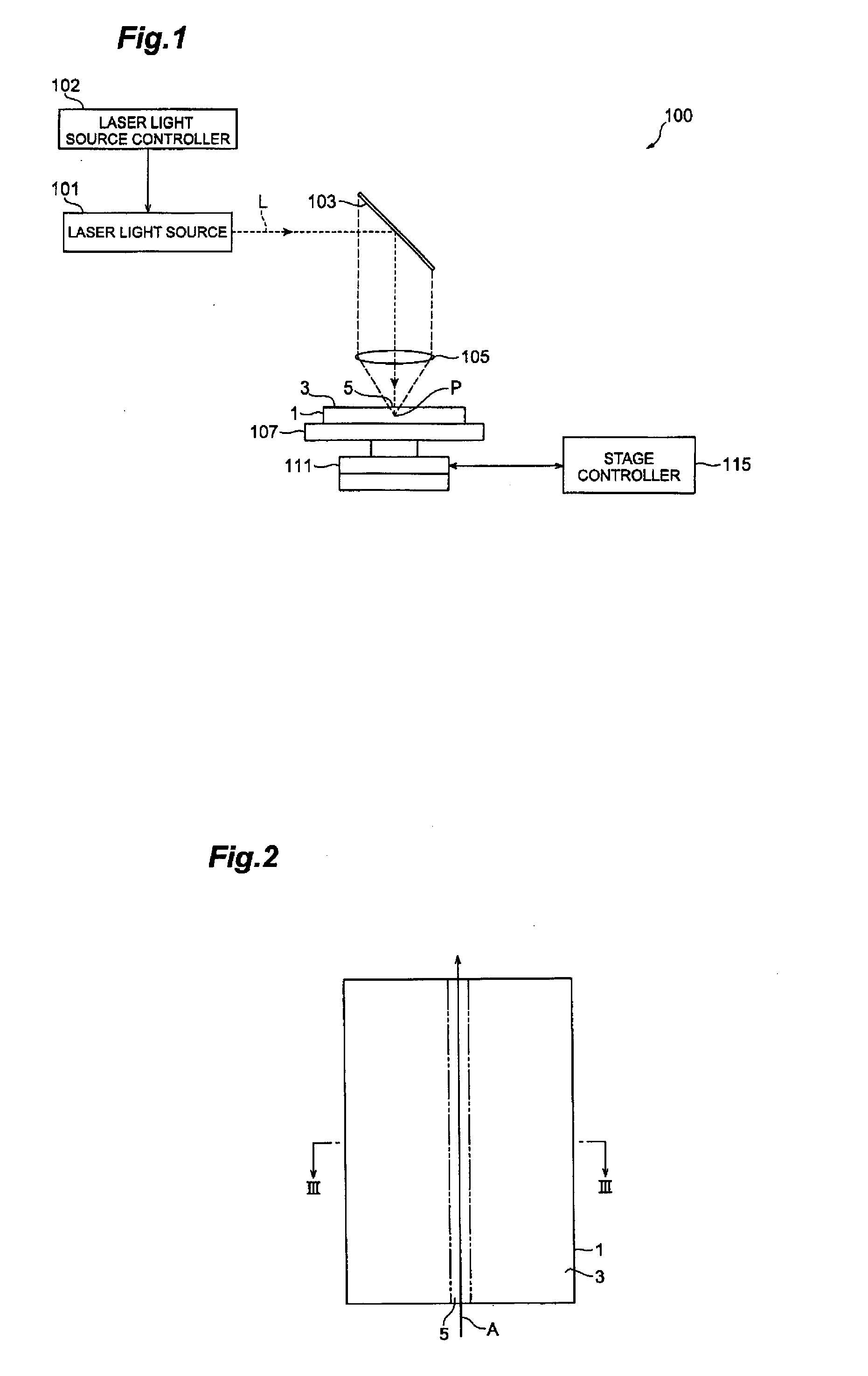
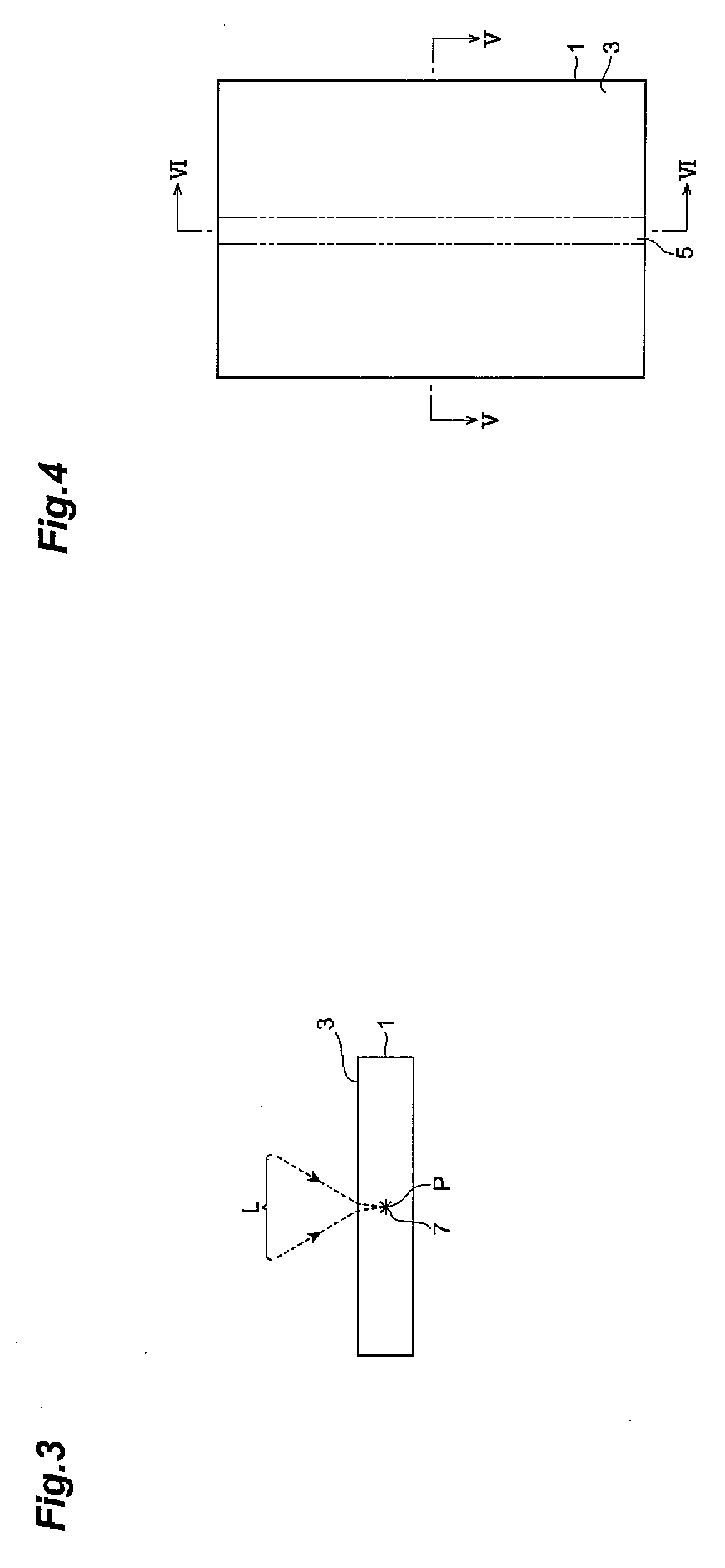
[0097]First, as shown in FIG. 19(a), an expandable tape (first sheet) 23 is attached to the rear face 21 of the object 1. Subsequently, the object 1 is secured onto a support table of a laser processing apparatus (not shown) such that the functional device layer 16 faces up. Then, as shown in FIG. 10, lines to cut 5 passing between the functional devices 15, 15 adjacent to each other are set like grids in directions perpendicular and parallel to the orientation flat 6.
[0098]Next, the object 1 is irradiated with the laser light L while using its front face 3 as a laser light entrance surface and locating the converging point P within the silicon wafer 1...
PUM
| Property | Measurement | Unit |
|---|---|---|
| Polarity | aaaaa | aaaaa |
| Electric charge | aaaaa | aaaaa |
| Area | aaaaa | aaaaa |
Abstract
Description
Claims
Application Information