

Packaged Microchip with Spacer for Mitigating Electrical Leakage Between Components
a technology of microchips and spacers, applied in the field of packaged microchips, can solve problems such as leakage current, die attaching material hardening, and prone to developing voids, and achieve the effect of preventing leakage curren
- Summary
- Abstract
- Description
- Claims
- Application Information
AI Technical Summary
Benefits of technology
Problems solved by technology
Method used
Image

Examples
Embodiment Construction
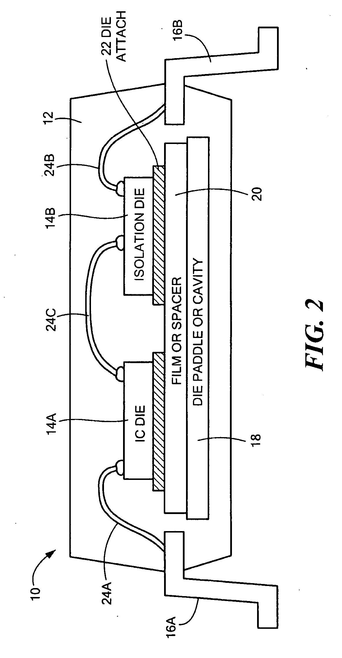
[0016]In illustrative embodiments, an insulative spacer substantially eliminates leakage currents between microchips within a package. Accordingly, use of the spacer should eliminate the need for complicated and expensive split paddle designs, or other schemes for mitigating leakage currents. Details of illustrative embodiments are discussed below.
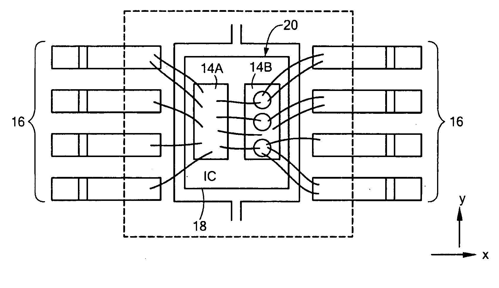
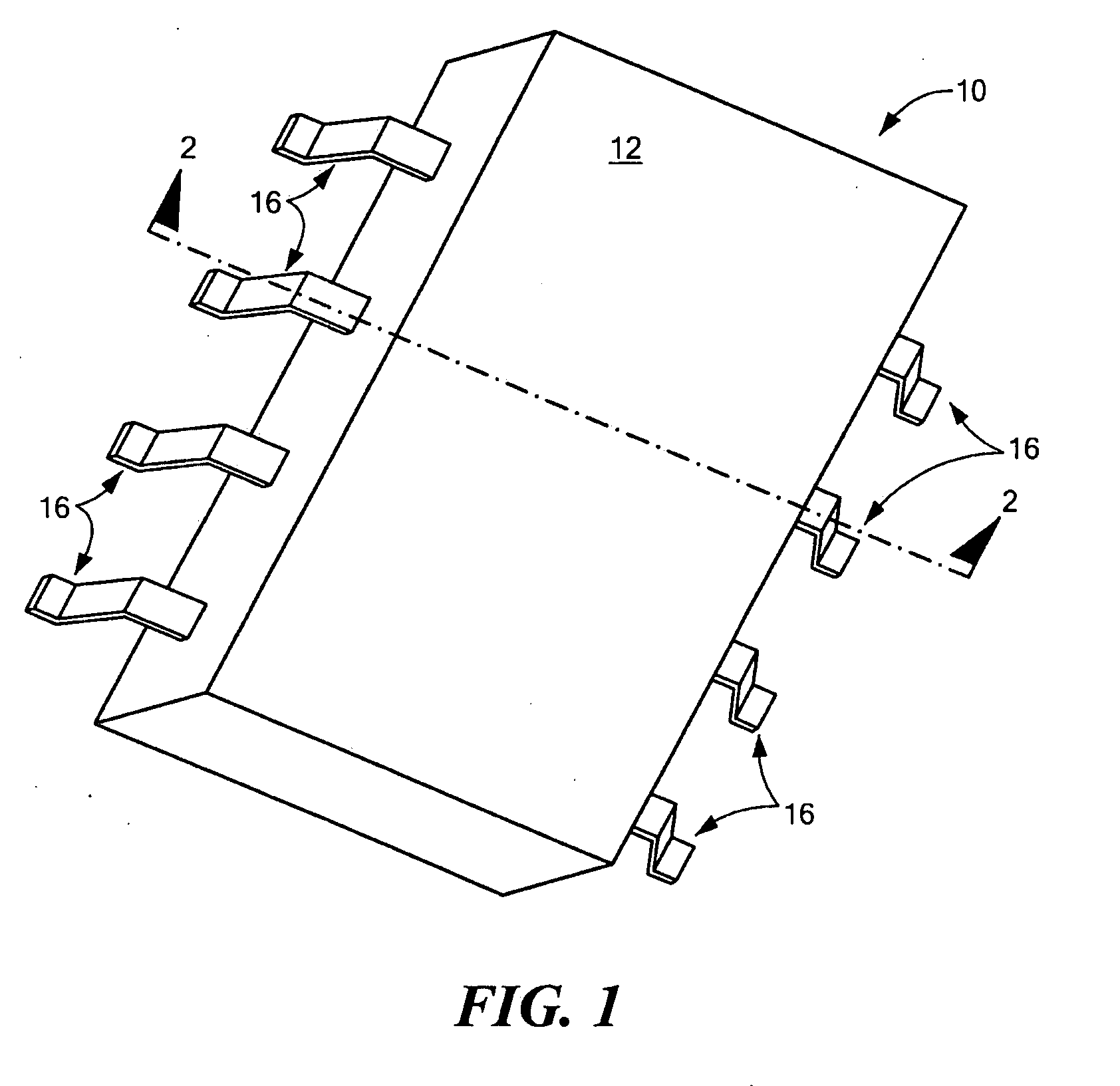
[0017]FIG. 1 schematically shows a perspective view of a packaged microchip 10 that may be configured in accordance with illustrative embodiments of the invention. The packaged microchip 10 shown has a postmolded leadframe package 12, commonly referred to as a “plastic package,” containing a plurality of microchips 14A and 14B (not shown in FIG. 1, but shown in FIGS. 2 and 3). The microchips 14A and 14B electrically communicate with exterior components by means of eight pins / leads 16 extending from the package 12. In one embodiment, one of the microchips may be an isolation circuit that provides electrical isolation against stray currents....
PUM
 Abstract
Description
Claims
Application Information