Liquid crystal display panel driving method, liquid crystal display device, and LCD driver
a technology of liquid crystal display device and driving method, which is applied in the direction of electric digital data processing, instruments, computing, etc., can solve the problems of increasing the power consumption of the liquid crystal display device, requiring large power for driving the counter electrode, and flickering to become apparent, so as to achieve the effect of reducing the power required
- Summary
- Abstract
- Description
- Claims
- Application Information
AI Technical Summary
Benefits of technology
Problems solved by technology
Method used
Image
Examples
first embodiment
[Structure of Liquid Crystal Display Device]
[0096]FIG. 6A is a block diagram showing a structure of a liquid crystal display device 1 according to a first embodiment of the present invention. The liquid crystal display device of a first embodiment includes an LCD panel 2 and an LCD driver 3. The LCD driver 3 includes a power supply circuit 11, a source driver circuit 12, a gate driver circuit 13, a VCOM circuit 14, and a timing control circuit 15.
[0097]The power supply circuit 11 generates supply voltages with voltage levels corresponding to each circuit from a power supply voltage VCI that is supplied form a VCI power supply interconnection 30. The VCI power supply interconnection 30 is an interconnection for supplying the power supply voltage VCI to the power supply circuit 11 from a VCI power supply (not shown). The VCI power supply may be integrated to the LCD driver or may be provided externally.
[0098]More specifically, the power supply circuit 11 supplies a power supply voltag...
second embodiment
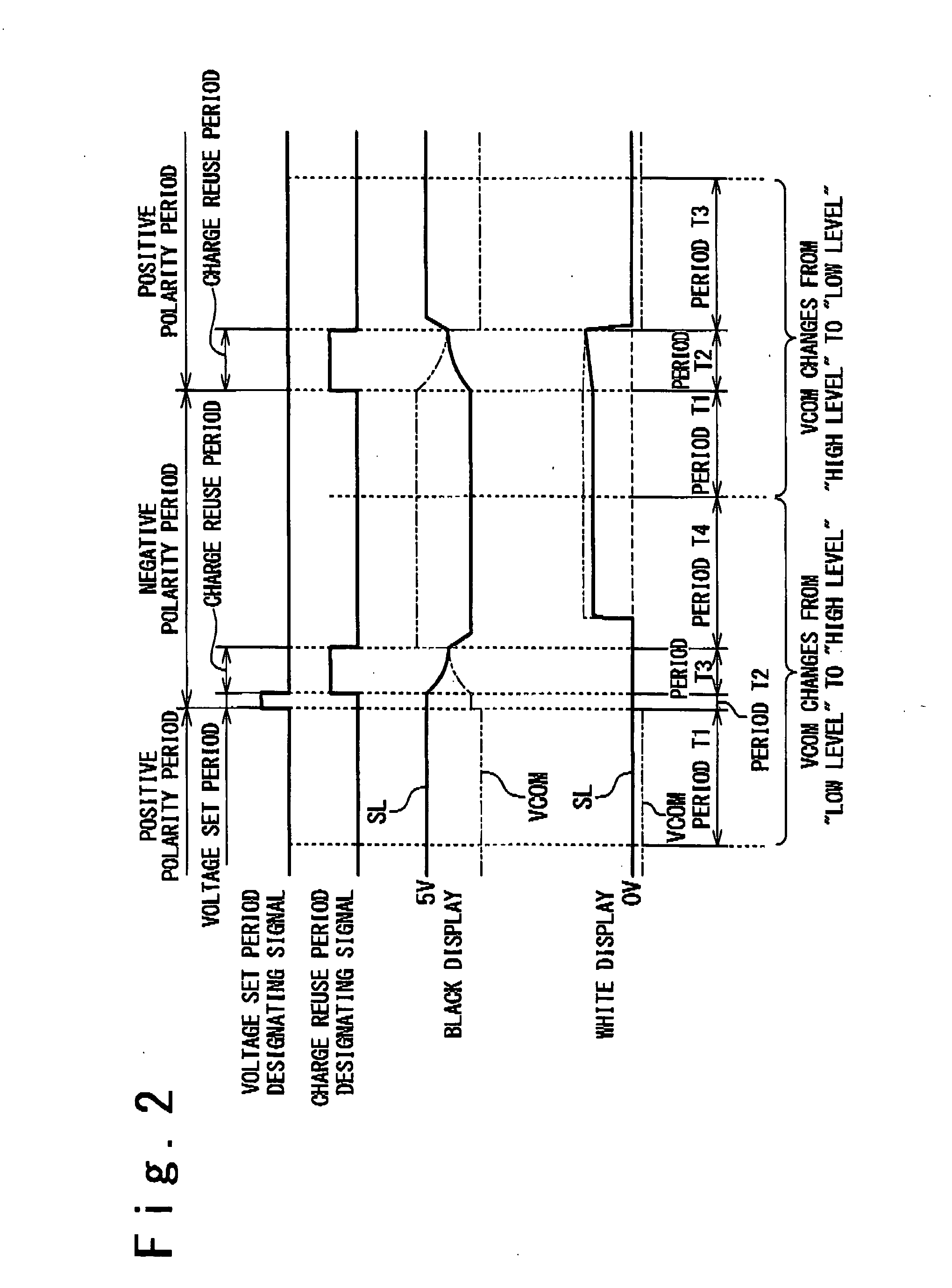
[0161]FIG. 25 is a timing chart for describing operations of the liquid crystal display device 1 according to a second embodiment when changing the polarity of the driving voltage from negative to positive, i.e., when pulling down the counter electrode VCOM from the potential VCOMH to the potential VCOML. FIG. 26 is a flowchart showing the operation of the liquid crystal display device 1 in each period. In a second embodiment, the counter electrode VCOM is pulled down to the potential VCOML by a procedure different from that of a first embodiment.
[0162]More specifically, the operations regarding the periods T1 to T3 of a second embodiment shown in FIGS. 25 and 26 are the same as the operations of a first embodiment shown in FIGS. 7A and 8A. In the period T1 under the initial state, the counter electrode VCOM is pulled up to the potential VCOMH, while the source lines S1 to Sn are driven to the potential corresponding to the image data. In the period T2 following the period T1, the s...
third embodiment
[0170]By comparing the electric charges consumed in the operations of a first embodiment for changing the polarity of the driving voltage from negative to positive, i.e., the electric charges consumed in the operations for pulling down the counter electrode VCOM to the potential VCOML (see FIG. 14), with the electric charges consumed by the same operations of a second embodiment (see FIG. 28), it can be understood that: for performing white display, the electric charge consumption is smaller in a first embodiment; and for performing black display, it is smaller in a second embodiment. Therefore, it is possible to reduce the electric charge consumption by changing, in accordance with the values of image data, the operation of the period T4 where the counter electrode VCOM is pulled down from the ground potential VSS to the potential VCOML.
[0171]More specifically, as shown in FIGS. 7A and 8A of a first embodiment, the source line Sj providing white display (that is, the source line Sj...
PUM
 Abstract
Description
Claims
Application Information


