Modular Chip Integration Techniques

a module chip and integrated chip technology, applied in the field of module chip integration and operation techniques, can solve the problems of chip scale technology, power consumption is a growing concern, and the effect of modular chip fabrication

Active Publication Date: 2009-04-30
IBM CORP
View PDF7 Cites 11 Cited by
  • Summary
  • Abstract
  • Description
  • Claims
  • Application Information

AI Technical Summary

Problems solved by technology

With an estimated $2.7 billion spent in 2005 to run servers and other associated computer equipment in the United States alone, power consumption is a growing concern.
These rapid advances in chip scale technology, however, can have notable drawbacks with regard to modular chip fabrication.
Namely, as chip technology changes, incompatibilities can often arise between the ‘old’ and the ‘new’ technologies.
Different power requirements can render one component incompatible with another component.
Thus, the versatility of current chip design technology can be limited unless all of the components are redesigned into the latest node for a new chip and fabricated using the scaled down features associated with the latest node of semiconductor wafers.

Method used


Image

  • Modular Chip Integration Techniques
  • Modular Chip Integration Techniques
  • Modular Chip Integration Techniques

Examples


Embodiment Construction

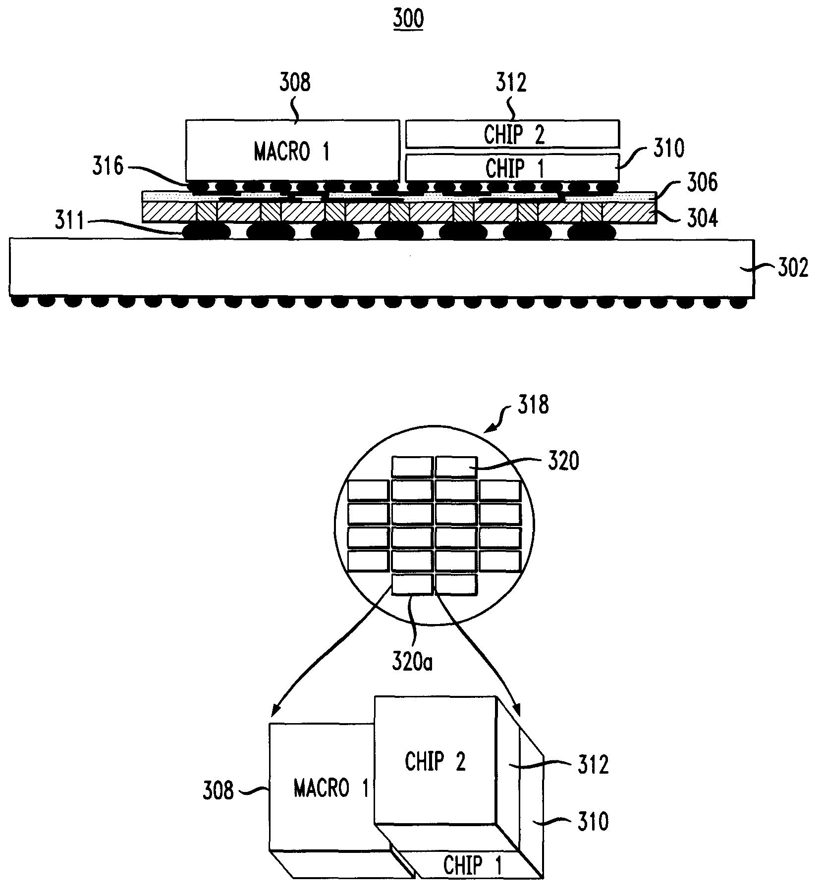
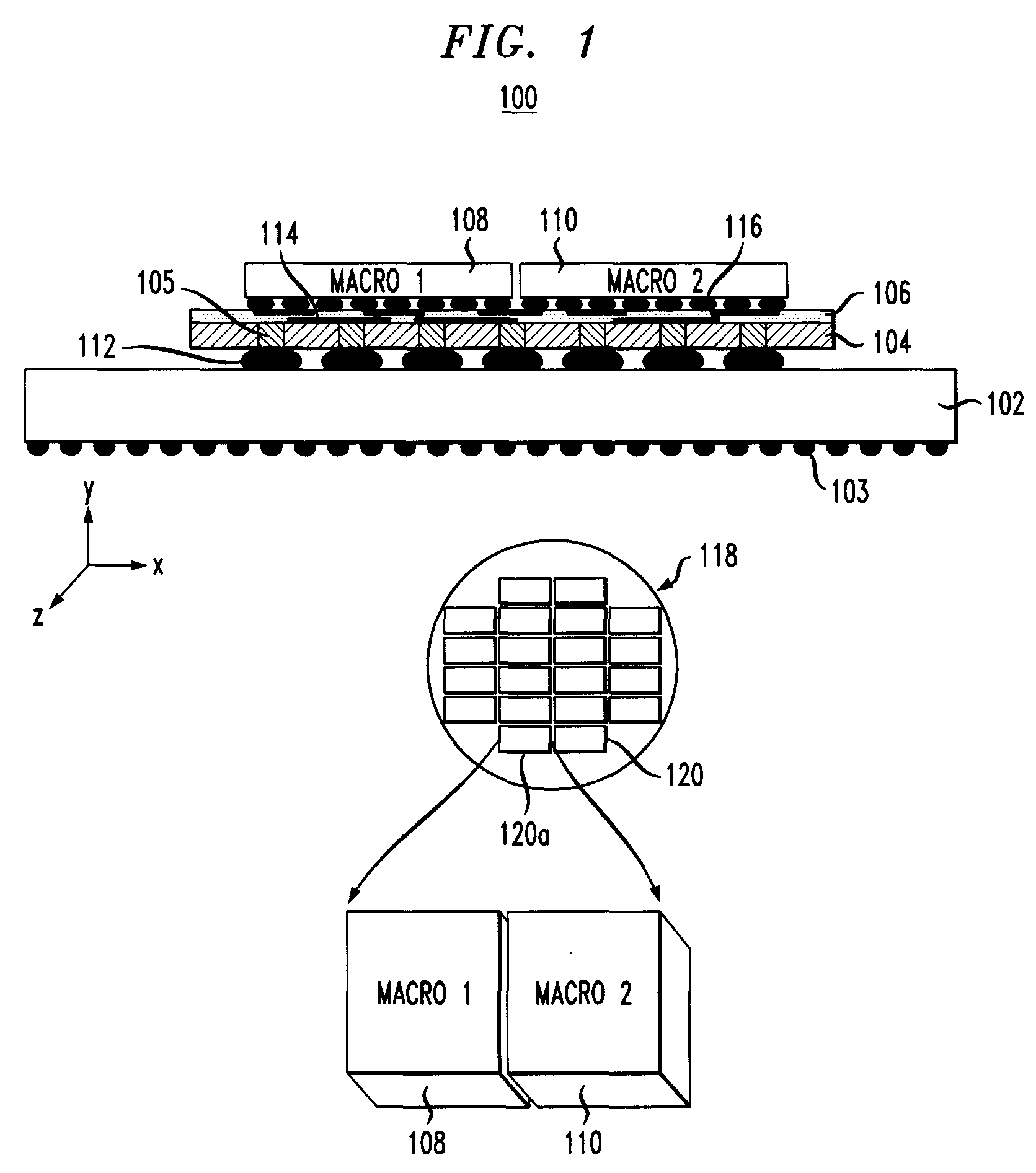
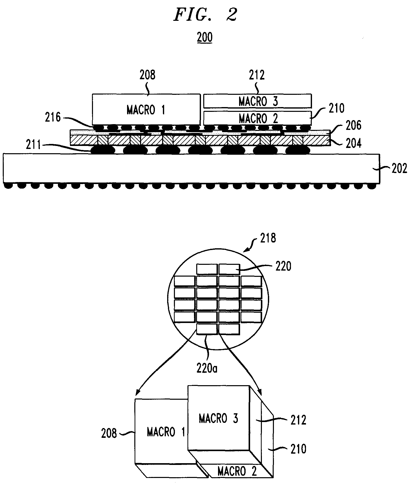
[0017]FIG. 1 is a diagram illustrating exemplary modular chip structure 100. Modular chip structure 100 may comprise, for example, a modular application specific integrated circuit (ASIC) structure. ASIC refers generally herein to any integrated circuit (chip) designed for a specific application, and includes, for example, custom and standard ASICs, such as system on a chip (SoC) designs.

[0018]As will be described in detail below, the present invention provides improved modular chip fabrication techniques that permit one or more pre-designed chip circuits, such as chips and / or chip macros (described below), to be used in modular form in conjunction with newly designed chips and / or chip macros (e.g., which collectively can support a new application) and / or with other pre-designed chips and / or chip macros, e.g., from a different node of semiconductor technology. Namely, the present techniques permit the integration of heterogeneous chip technology, reuse of chip designs and macros and...


PUM


Abstract

Modular chip integration and operation techniques are provided. In one aspect, a method of integrating chips, chip macros or at least one chip in combination with at least one chip macro is provided. The method comprises the following steps. The chips, chip macros or at least one chip in combination with at least one chip macro are assembled on a single carrier platform. One or more signal inputs and outputs are provided to each of the chips, chip macros or at least one chip in combination with at least one chip macro. One or more power and ground inputs and outputs are provided to each of the chips, chip macros or at least one chip in combination with at least one chip macro. The power and ground inputs and outputs to one or more of the chips, chip macros or at least one chip in combination with at least one chip macro are segmented from the power and ground inputs and outputs to at least one other of the chips, chip macros or at least one chip in combination with at least one chip macro so as to form a plurality of voltage islands.

Description

CROSS-REFERENCE TO RELATED APPLICATIONS[0001]This application is related to the commonly owned U.S. application Ser. No. 11 / 929,335, entitled “Techniques for Modular Chip Fabrication,” designated as Attorney Reference Number YOR920070187US1, filed herewith on the same day of Oct. 30, 2007, the contents of which are incorporated herein by reference.FIELD OF THE INVENTION[0002]The present invention relates to chip design, and more particularly, to modular chip integration and operation techniques.BACKGROUND OF THE INVENTION[0003]When developing new chip designs, it is common for chip designers to combine pre-designed components to form the new chip. This modular chip fabrication process is beneficial as it takes advantage of preexisting proven technology. For example, a chip designer might combine components from several different previously developed chips.[0004]The computer chip industry is constantly developing and employing process technologies to produce chips having smaller feat...

Claims


Application Information

Patent Timeline
Patent Type & Authority Applications(United States)
IPC IPC(8): H01L21/50
CPCH01L23/49827H01L2224/16H01L24/16H01L24/81H01L25/0652H01L2224/13147H01L2224/73204H01L2224/81193H01L2224/81815H01L2224/8185H01L2224/81895H01L2224/831H01L2924/01013H01L2924/01029H01L2924/01032H01L2924/01049H01L2924/01073H01L2924/01078H01L2924/01082H01L2924/01322H01L2924/04941H01L2924/09701H01L2924/13091H01L2924/14H01L2924/1433H01L2924/15311H01L2924/19041H01L2924/19043H01L2924/19105H01L23/60H01L2924/00014H01L2924/01015H01L2924/10253H01L2924/15192H01L2224/16225H01L2224/45147H01L2924/10329H01L2924/01075H01L2924/01074H01L2924/01006H01L2924/01021H01L2924/01023H01L2924/01033H01L2924/01047H01L2924/0105H01L2924/00H01L2224/48
Inventor CARON, ALAINKNICKERBOCKER, JOHN ULRICH
Owner IBM CORP
Why Eureka
Try Eureka