Memory module and control method of serial peripheral interface using address cache
- Summary
- Abstract
- Description
- Claims
- Application Information
AI Technical Summary
Benefits of technology
Problems solved by technology
Method used
Image


Examples
Embodiment Construction
[0020]The present invention will be described with reference to the accompanying drawings.
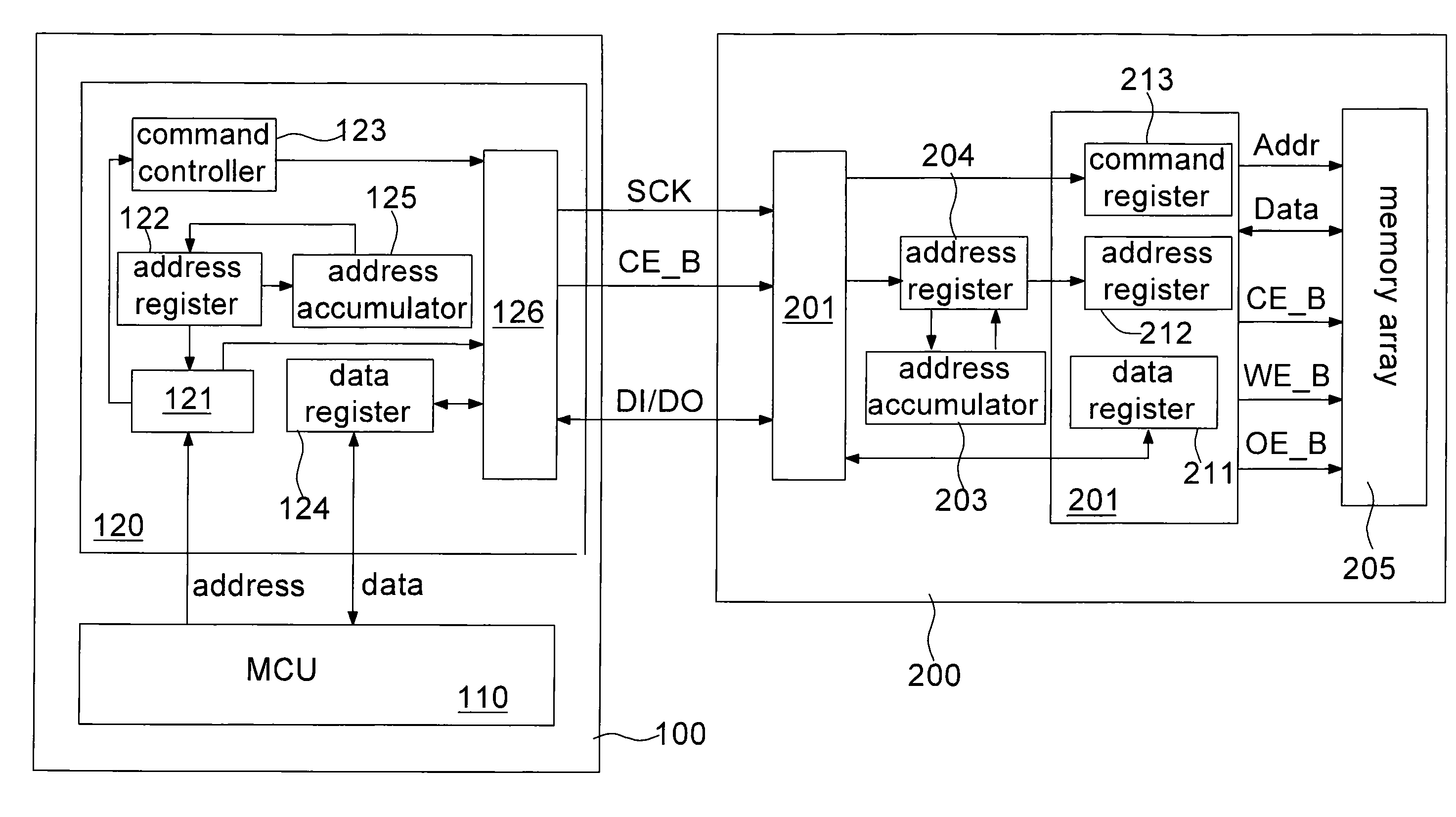
[0021]FIG. 2 is a block diagram of a SPI memory system using address cache according to an embodiment of the present invention. As shown in FIG. 2, a SPI memory system using address cache comprises a system chip 100 and a flash memory module 200. When the system chip 100 receives an access command of memory data, it performs data access to the flash memory module 200. The system chip 100 is coupled to the flash memory module 200 by means of a plurality of input / output ports (I / O ports). The I / O ports include a system reference clock SCK, a chip select signal CE_B, a plurality of data signals DI, DO and so forth. Here, the plurality of data signals DI, DO are transmitted in serial form. The system chip 100 includes a micro-controller unit (MCU) 110 and a SPI controller 120. The SPI controller 120 includes a serial / parallel converter 126, a data register 124, a command controller 123, an address ...
PUM
 Abstract
Description
Claims
Application Information