Phosphor surface treating method and flat display device manufacturing method
a technology of phosphor surface and manufacturing method, which is applied in the direction of pretreated surfaces, coatings, electric discharge tubes, etc., can solve the problems of low current density obtained by electron beams, inability to obtain inability to obtain a sufficient light emission luminance and sufficient life, etc., to achieve simple and inexpensive manufacturing
- Summary
- Abstract
- Description
- Claims
- Application Information
AI Technical Summary
Benefits of technology
Problems solved by technology
Method used
Image

Examples
example 1
Formation of Sample for Measuring Light Emission Characteristics
[0060]10 g of an 8-wt % solution of octylic acid La manufactured by NIHON KAGAKU SANGYO was added to 490 g of Isopar L (registered trademark) manufactured by Exxon, and the mixture was stirred for 30 min by a stirrer, thereby obtaining an octylic acid La solution. 50 g of a ZnS:Ag,Al blue emitting phosphor was added to the octylic acid La solution, and the mixture was stirred for 2 hrs by the stirrer, thereby performing a surface treatment by which octylic acid La was adhered to the surface of the ZnS:Ag,Al phosphor.
[0061]31.25 g of the surface-treated ZnS:Ag,Al phosphor and 18.75 g of an ethylcellulose resin for screen printing were stirred by the stirrer, thereby preparing screen printing paste weighing 50 g.
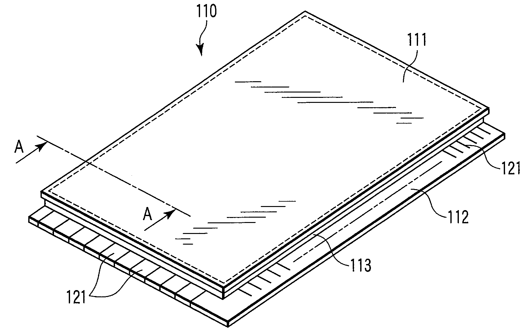
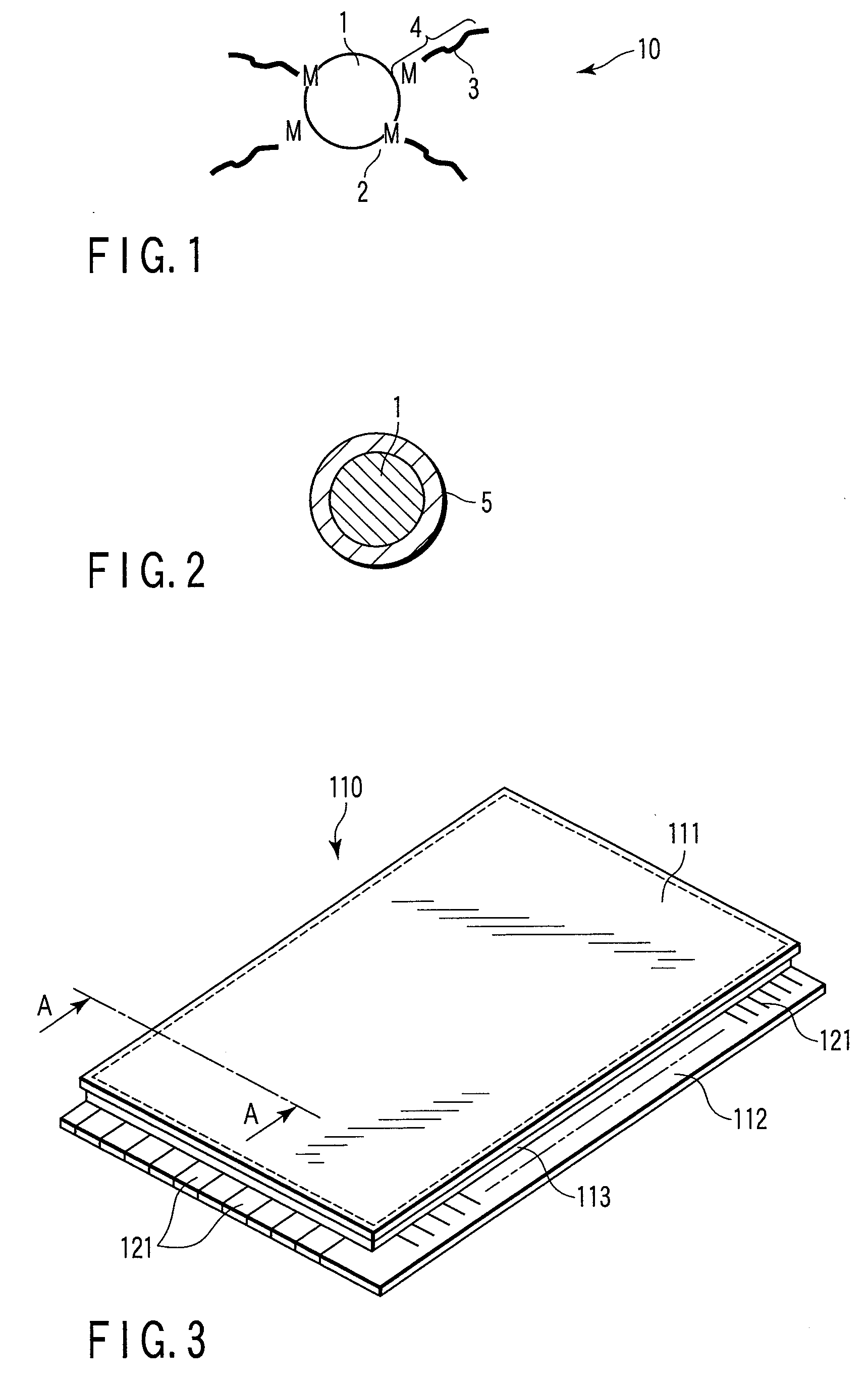
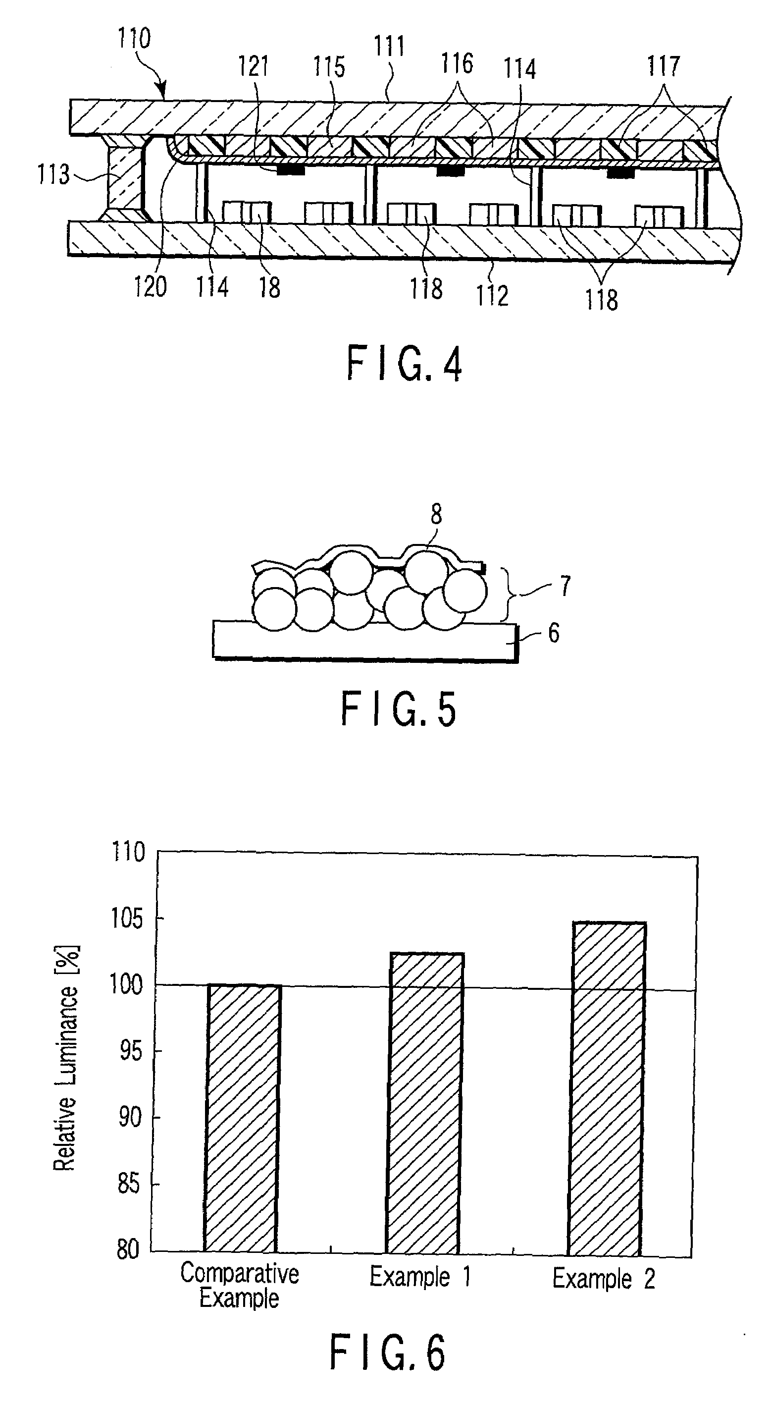
[0062]FIG. 5 is a model view showing a sample for measuring the light emission characteristics.
[0063]The screen printing paste prepared as described above was used to form a phosphor layer 7 about 10 μm thick on a...
example 2
[0067]20 g of a 3-wt % solution of octylic acid Mg manufactured by NIHON KAGAKU SANGYO was added to 480 g of Isopar L (registered trademark) manufactured by Exxon, and the mixture was stirred for 30 min by a stirrer, thereby obtaining an octylic acid Mg solution. 50 g of a ZnS:Ag,Al blue phosphor was added to the octylic acid Mg solution, and the mixture was stirred for 2 hrs by the stirrer, thereby performing a surface treatment by which octylic acid Mg was adhered to the surface of the ZnS:Ag,Al phosphor.
[0068]31.25 g of the surface-treated ZnS:Ag,Al phosphor and 18.75 g of an ethylcellulose resin for screen printing were stirred by the stirrer, thereby preparing a screen printing paste weighing 50 g.
[0069]The screen printing paste prepared as described above was used to form a phosphor layer 7 about 10 μm thick on a glass substrate 6 (100 mm×100 mm) by screen printing. A metal back layer 8 about 120 nm thick was formed on the upper surface of the phosphor layer 7 by vapor deposit...
example 3
[0077]31.25 g of a ZnS:Ag,Al phosphor, 15.13 g of an ethylcellulose resin for screen printing, and 3.12 g of an 8-wt % solution of octylic acid La manufactured by NIHON KAGAKU SANGYO were mixed, and the mixture was stirred by a stirrer, thereby preparing screen printing paste weighing 50 g.
[0078]The screen printing paste prepared as described above was used to form a phosphor layer 7 about 10 μm thick on a glass substrate 6 (100 mm×100 mm) by screen printing. A metal back layer 8 about 120 nm thick was formed on the upper surface of the phosphor layer 7 by vapor deposition of Al, and annealing was performed at 500° C. for 30 min, thereby forming a sample for measuring the light emission characteristics as shown in FIG. 5.
[0079]The light emission luminance and light emission life were evaluated by irradiating an electron beam at an acceleration voltage of 10 kV and a current density of 3.6 mA / cm2 (electric current=250 μA, and raster size=10 mm×70 mm) at the sample shown in FIG. 5, to...
PUM
 Abstract
Description
Claims
Application Information
 - R&D
- Intellectual Property
- Life Sciences
- Materials
- Tech Scout
- Unparalleled Data Quality
- Higher Quality Content
- 60% Fewer Hallucinations
Browse by: Latest US Patents, China's latest patents, Technical Efficacy Thesaurus, Application Domain, Technology Topic, Popular Technical Reports.
© 2025 PatSnap. All rights reserved.Legal|Privacy policy|Modern Slavery Act Transparency Statement|Sitemap|About US| Contact US: help@patsnap.com