Method and apparatus for forming copper indium gallium chalcogenide layers

a technology of which is applied in the field of methods and apparatus for forming copper indium gallium chalcogenide layers, can solve the problems of reducing device efficiency, reducing the electronic quality of cigs material, and increasing the performance of silicon-based solar cells. , to achieve the effect of improving the performance of such absorbers and reducing the efficiencies

Inactive Publication Date: 2009-05-07
SOLOPOWER
View PDF19 Cites 21 Cited by
  • Summary
  • Abstract
  • Description
  • Claims
  • Application Information

AI Technical Summary

Problems solved by technology

However, the cost of electricity generated using silicon-based solar cells is higher than the cost of electricity generated by the more traditional methods.
When this ratio increases further, the device efficiency gets reduced.
Although the reasons for this are not fully understood, it is reported that the electronic quality of CIGS material gets worse as the Ga / (Ga+In) ratio increases beyond 0.3.
Although CIS formation using two-stage processes is rather straight forward, complications arise when Ga is added to be able to form a CIGS absorber.
As can be seen from this figure, one problem faced with the selenization type or two-stage processes is the difficulty to distribute Ga uniformly through the thickness of the absorber layer formed after reaction of Cu, In and Ga containing metallic precursor film with Se.
Therefore, such a process yields compound absorber layers with surfaces that are rich in In and poor in Ga.

Method used


Image

  • Method and apparatus for forming copper indium gallium chalcogenide layers
  • Method and apparatus for forming copper indium gallium chalcogenide layers
  • Method and apparatus for forming copper indium gallium chalcogenide layers

Examples


Embodiment Construction

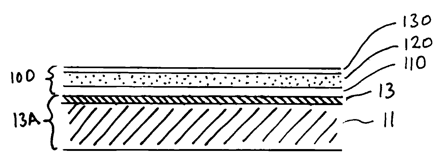
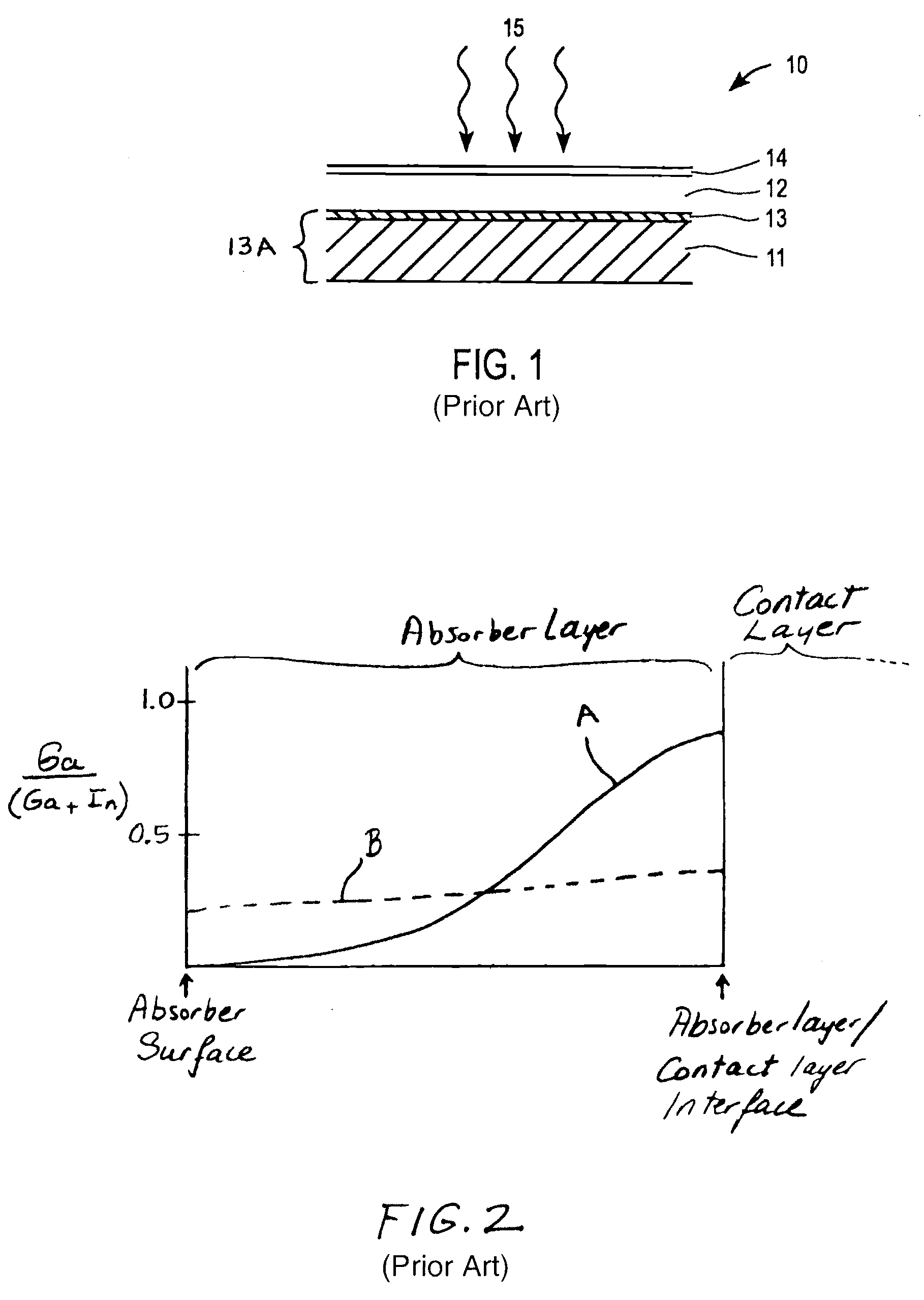
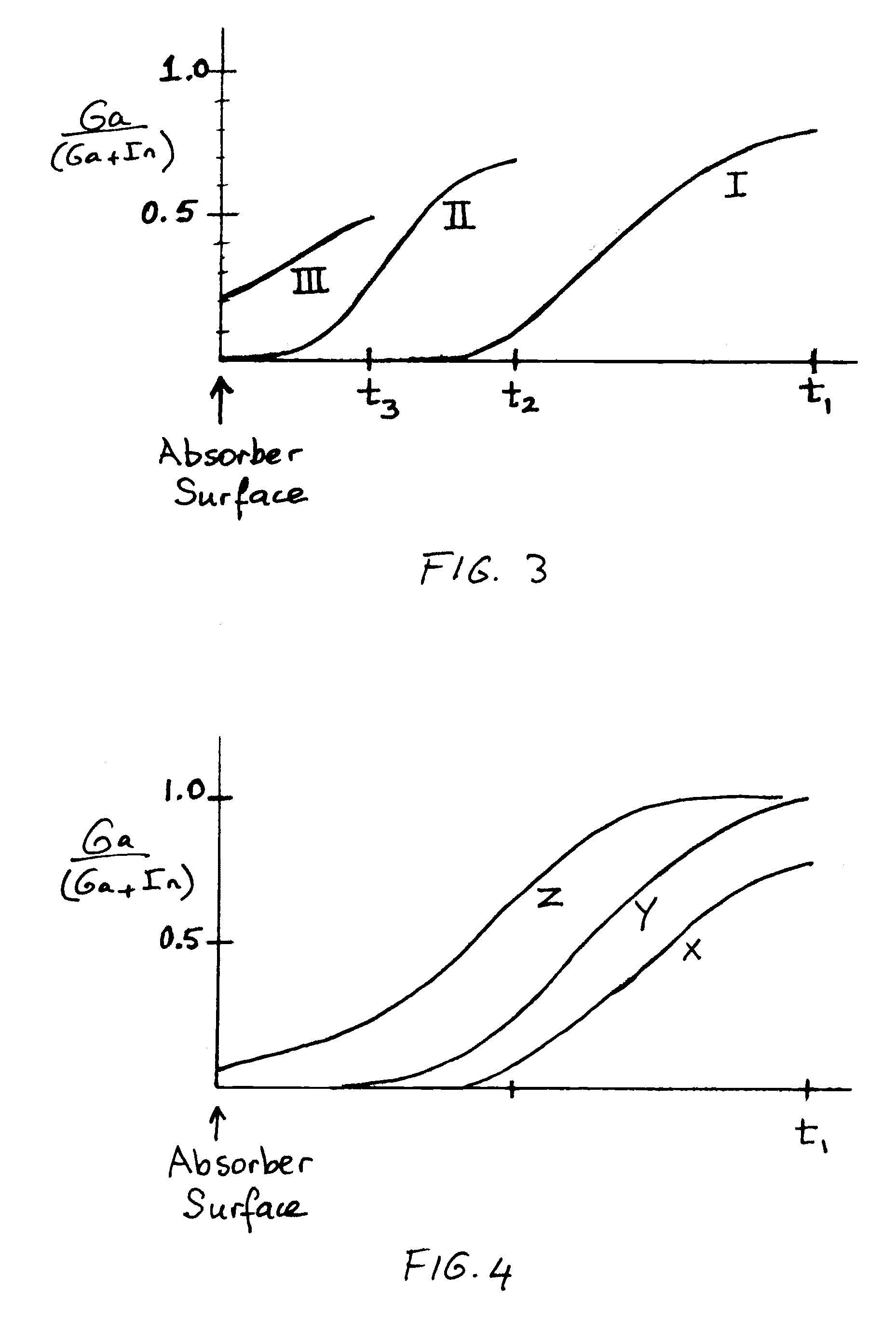
[0023]Present invention provides a method of making a multilayer structure for manufacturing solar cell absorbers. The multilayer structure may be built on a continuous flexible foil or workpiece which is suitable for roll-to-roll or reel-to-reel manufacturing processes, i.e., feeding the continuous substrate from a supply roll into the process tool that manufactures the multilayer structure and taking up and wrapping the finished product around a take-up roll.

[0024]In a first embodiment the method includes forming a first layer of a precursor stack on a conductive contact layer of the continuous workpiece which may be a metallic foil. The first layer may include a gallium-indium-selenide compound layer with a gallium to indium ratio of 0-0.8. On the first layer, a metallic layer including copper, gallium and indium metals is formed. In the metallic layer, gallium to indium ratio may be in the range of 0.2-0.3. After preparing the precursor stack another layer of selenium may be add...


PUM

PropertyMeasurementUnit
molar ratioaaaaaaaaaa

Abstract

A multilayer structure to form absorber layers for solar cells. The multilayer structure includes a base comprising a contact layer on a substrate layer, a first layer on the contact layer, and a metallic layer on the first layer. The first layer includes an indium-gallium-selenide film and the gallium to indium molar ratio of the indium-gallium-selenide film is in the range of 0 to 0.8. The metallic layer includes gallium and indium without selenium. Additional selenium is deposited onto the metallic layer before annealing the structure for forming an absorber.

Description

[0001]This application claims priority to U.S. Provisional Application Ser. No. 60 / 983,045, filed Oct. 26, 2007, entitled “Method and Apparatus for Forming Copper Indium Gallium Chalcogenide Layers”, which application is expressly incorporated by reference herein.[0002]The present invention relates to method and apparatus for preparing thin films of semiconductor films for radiation detector and photovoltaic applications.FIELD OF THE INVENTIONBackground[0003]Solar cells are photovoltaic devices that convert sunlight directly into electrical power. The most common solar cell material is silicon, which is in the form of single or polycrystalline wafers. However, the cost of electricity generated using silicon-based solar cells is higher than the cost of electricity generated by the more traditional methods. Therefore, since early 1970's there has been an effort to reduce cost of solar cells for terrestrial use. One way of reducing the cost of solar cells is to develop low-cost thin fi...

Claims


Application Information

Patent Timeline
Patent Type & Authority Applications(United States)
IPC IPC(8): H01L31/0272H01L31/18
CPCY02E10/541H01L31/0322Y02P70/50
Inventor BASOL, BULENT M.
Owner SOLOPOWER
Why Eureka
Try Eureka