Wire bond free wafer level LED

a technology of wire bonding and wafers, applied in the field of semiconductor/solid-state device manufacturing, semiconductor devices, electrical apparatus, etc., can solve the problem of limited external quantum efficiency

Active Publication Date: 2009-05-14
CREELED INC
View PDF84 Cites 151 Cited by
  • Summary
  • Abstract
  • Description
  • Claims
  • Application Information

AI Technical Summary

Problems solved by technology

For conventional LEDs with a single out-coupling surface, the external quantum efficiency is limited by total internal reflection (TIR) of light from the LED's emission region that passes through the substrate.
One disadvantage inherent to all of these exemplary configurations is that their design prevents package level components such as, for example, a phosphor layer or an encapsulation structure from being applied until after the device is singulated and mounted in a conventional LED package.
In some cases the constraint is caused by the need to connect the device to an outside voltage source using a wire bond or other similar means of connection.

Method used


Image

  • Wire bond free wafer level LED
  • Wire bond free wafer level LED
  • Wire bond free wafer level LED

Examples


Embodiment Construction

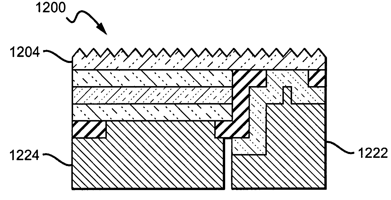
[0035]The present invention as embodied in the claims enables wafer-level packaging of semiconductor devices, such as high efficiency light emitting diode (LED) devices, for example. The claims also teach a method for fabricating these devices. Similarly as in other semiconductor devices, a bias voltage is applied across the device and light is emitted as a result of radiative recombination in the active region of the device. Various elements and procedures can be used to increase the light output of the device. For example, layers of materials functioning as mirrors or refractors can be formed at certain locations within the device to redirect emitted light away from photon absorbing materials such as the substrate. Another method often employed in the art is to roughen or texture one or more of the layers to prevent total internal reflection. Such features are typically added at the wafer level of fabrication.

[0036]It is sometimes desirable to alter the emission spectrum of an LED...


PUM


Abstract

A wire-bond free semiconductor device with two electrodes both of which are accessible from the bottom side of the device. The device is fabricated with two electrodes that are electrically connected to the oppositely doped epitaxial layers, each of these electrodes having leads with bottom-side access points. This structure allows the device to be biased with an external voltage/current source, obviating the need for wire-bonds or other such connection mechanisms that must be formed at the packaging level. Thus, features that are traditionally added to the device at the packaging level (e.g., phosphor layers or encapsulants) may be included in the wafer level fabrication process. Additionally, the bottom-side electrodes are thick enough to provide primary structural support to the device, eliminating the need to leave the growth substrate as part of the finished device.

Description

[0001]This invention was made with Government support under Contract No. 70NANB4H3037 of the Department of Commerce. The Government has certain rights in this invention.BACKGROUND OF THE INVENTION[0002]1. Field of the Invention[0003]This invention relates to semiconductor devices, and in particular to light emitting devices capable of wire bond free fabrication and operation.[0004]2. Description of the Related Art[0005]Light emitting diodes (LED or LEDs) are solid state devices that convert electric energy to light, and generally comprise one or more active layers of semiconductor material sandwiched between oppositely doped layers. When a bias is applied across the doped layers, holes and electrons are injected into the active layer where they recombine to generate light. Light from the active layer is emitted from all surfaces of the LED.[0006]There has been a great deal of recent interest in LEDs formed of Group-III nitride based material systems because of their unique combinati...

Claims


Application Information

Patent Timeline
Patent Type & Authority Applications(United States)
IPC IPC(8): H01L33/00H01L33/38H01L33/48H01L33/50H01L33/60H01L33/62
CPCH01L33/22H01L33/385H01L33/486H01L33/62H01L2224/49107H01L2224/48091H01L33/46H01L2924/00014H01L2224/45139H01L2224/45099H01L2224/45015H01L2924/207H01L33/58H01L33/50H01L25/0756H01L33/08H01L33/505H01L2924/00
Inventor KELLER, BERNDCHITNIS, ASHAYMEDENDORP, JR., NICHOLAS W.IBBETSON, JAMESBATRES, MAX
Owner CREELED INC
Why Eureka
Try Eureka