Self-Aligning Structures and Method For Integrated Circuits

a technology of integrated circuits and structures, applied in the direction of electrical equipment, semiconductor devices, semiconductor/solid-state device details, etc., can solve problems such as product reliability problems, and achieve the effect of increasing the wettable surface area

Active Publication Date: 2009-05-14
INTERSIL INC
View PDF10 Cites 22 Cited by
  • Summary
  • Abstract
  • Description
  • Claims
  • Application Information

AI Technical Summary

Benefits of technology

[0007]A clip structure is mounted to a leadframe using a “tub” or trench-like formation that is formed in the leadframe material and shaped to receive or accept the geometric shape of the clip at the end thereof that connects to the leadframe. In the preferred embodiment, a leadframe structure is fabricated by etching with at least one portion thereof including a half-etch recess or tub or trench that receives one end of the clip structure and is temporarily retained in the tub by a selected quantity of solder paste or equivalent material. The end of the clip that is received in the tub is thus held in place in the x,y,z planes during subsequent handling until the clip and leadframe undergo solder reflow to effect an electrical connection and a corresponding mechanical connection. The tub and / or the clip include recesses or pockets that increase the wettable surface area on one side of the clip relative to the other side thereof. During the solder reflow step, the liquefied solder wets the increase surface area side of the clip with the tendency of liquid or molten solder to minimize its surface area causing the parts to draw to and toward their final as-designed alignment.

Problems solved by technology

As occasionally happens, the clip is mis-aligned during placement; in some cases the mis-aligned clip can contribute to product reliability issues.

Method used


Image

  • Self-Aligning Structures and Method For Integrated Circuits
  • Self-Aligning Structures and Method For Integrated Circuits
  • Self-Aligning Structures and Method For Integrated Circuits

Examples


Embodiment Construction

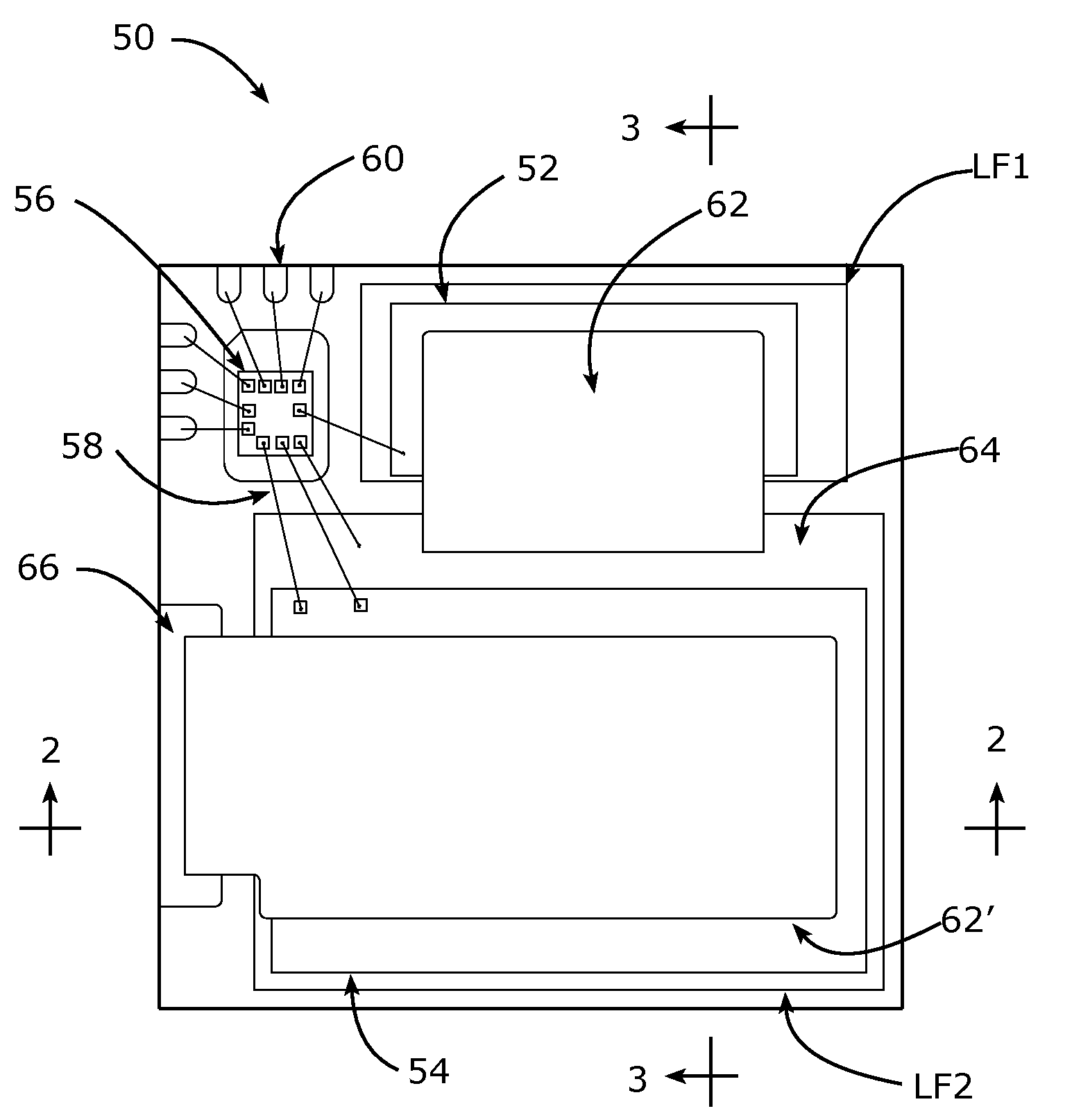
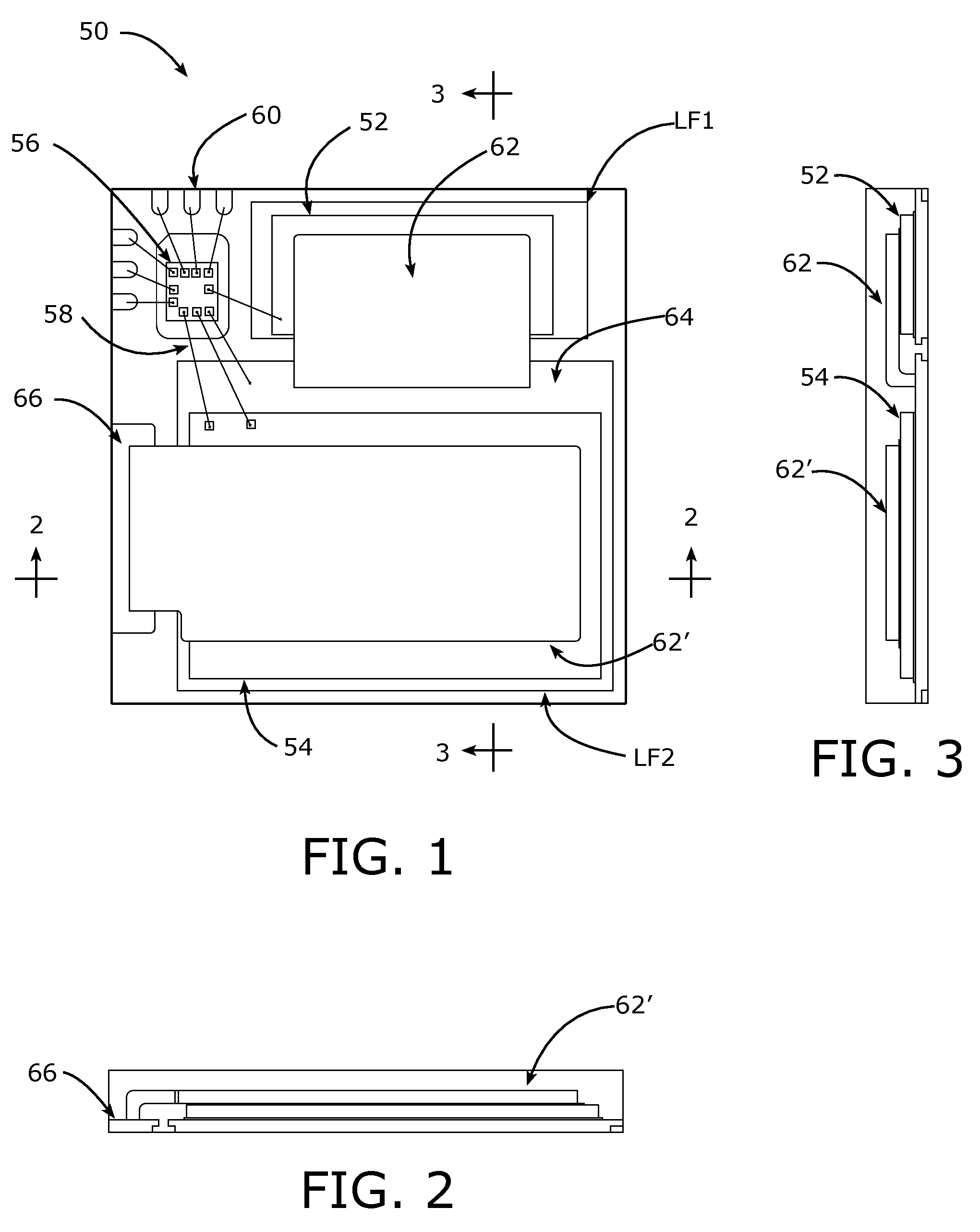
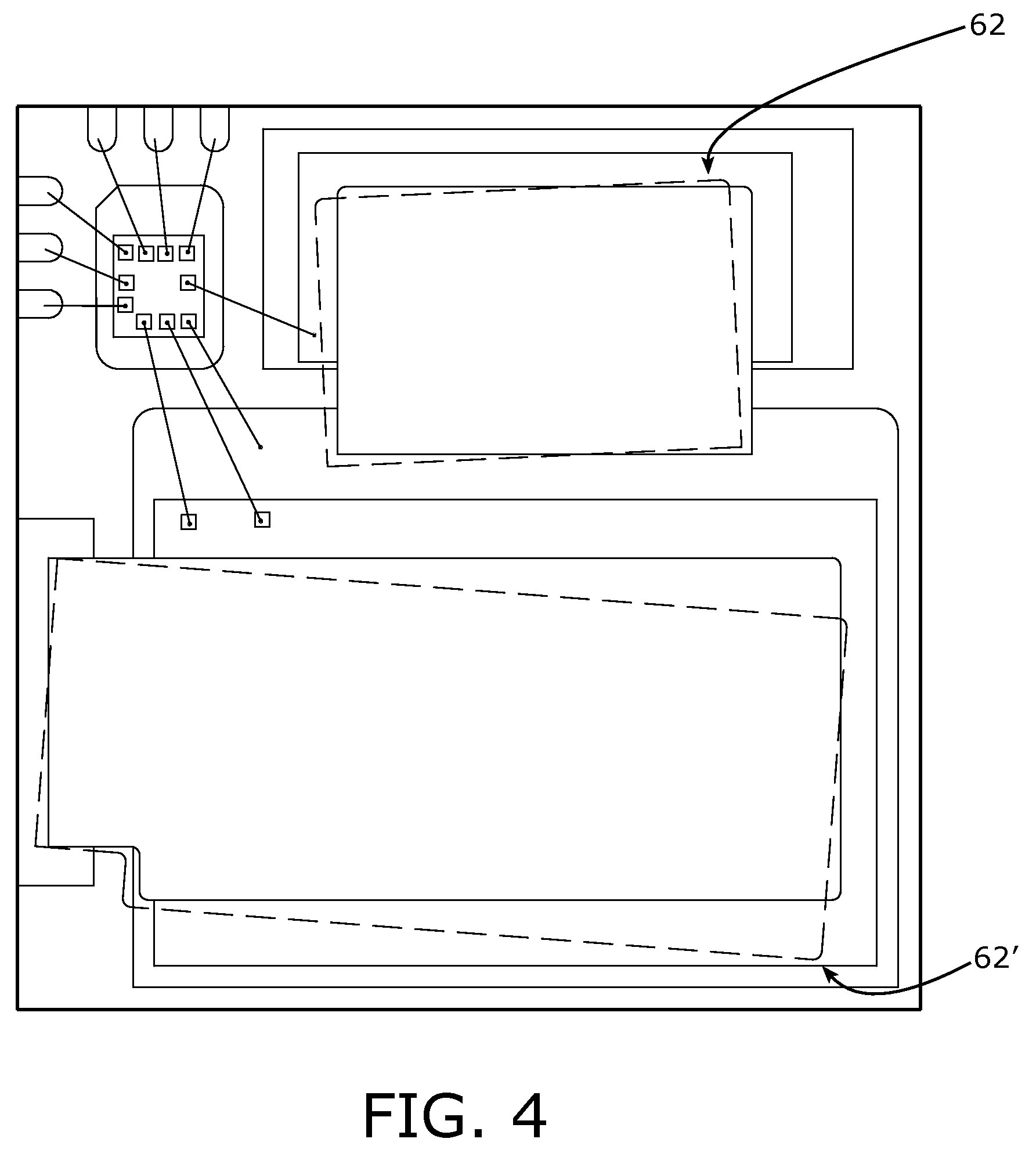
[0027]FIGS. 1-3 illustrate an example circuit assembly, designated generally by the reference character 50, and shows first and second FETs 52 and 54 mounted atop respective leadframes LF1 and LF2. A controller or driver chip 56 is connected via bonding wires 58 between conductive pads (unnumbered) on the driver chip 56 to contacts 60 and via bonding wires 58 connected to selected portions of the FETs 52 and 54. While each FET 52 / 54 is mounted on a respective leadframe LF1 / LF2 in FIG. 1a, both respective leadframes constitute a leadframe collectively for the assembly.

[0028]As shown, a conductive first clip 62 (typically fabricated from copper or a copper alloy) is connected between the top surface of the FET 52 and a surface portion 64 of the leadframe LF2 and second conductive clip 62′ is connected between the top surface of the FET 54 and another portion 66 of the leadframe.

[0029]As shown in FIGS. 2 and 3, the clips 62 and 62′ are fabricated as generally “L” shaped members with an...


PUM


Abstract

A lead frame having a die thereon connects a high current conductive area on the die to a lead frame contact using a copper clip that includes a structure portion that is received with a recess-like “tub” formed in the lead frame contact. In the preferred embodiment, a lead frame structure fabricated by etching includes at least one contact that is a half-etch recess or “tub” that receives one end of the clip structure and is retained in the tub by solder paste or an adhesive. The end of the clip that is received in the tub is held in place during subsequent handling until the clip and leadframe undergo solder reflow to effect an electrical connection sufficient to handle the current load and a also effect a reliable mechanical connection. One or more solder-holding pockets are formed a surface portion of the tub and/or the end of the clip that is received in the tub so that a volume of liquefied solder formed during the solder reflow step will effect alignment of any mis-aligned parts by “drawing” at least one of the parts against a “stop” surface.

Description

CROSS-REFERENCE TO RELATED APPLICATION[0001]This patent application claims the benefit of commonly owned U.S. Provisional Patent Application 60 / 990,280 filed Nov. 26, 2007 by the inventor herein and entitled “Self-Aligning Structures for Integrated Circuits,” the benefit of commonly owned U.S. Provisional Patent Application 60 / 986,579 filed Nov. 8, 2007 by the inventor herein and entitled “Clip Mount For Integrated Circuit Leadframes,” and the benefit of commonly owned U.S. patent application Ser. No. 12 / 250,525 filed Oct. 13, 2008 by the inventor herein and entitled “Clip Mount For Integrated Circuit Leadframes” the respective disclosures of which are incorporated herein by reference.BACKGROUND OF THE INVENTION[0002]The present invention relates to the improved placement and self-alignment of structures associated with an integrated circuit and, more particularly, to structures, including mechanical and electrical connection structures, designed to self-align into their as-designed...

Claims


Application Information

Patent Timeline
Patent Type & Authority Applications(United States)
IPC IPC(8): H01L21/60H01L23/495
CPCH01L2924/01029H01L2924/01074H01L2924/1306H01L2224/37147H01L2224/40247H01L2224/73221H01L2924/014H01L2924/01082H01L2924/13091H01L2924/14H01L23/49503H01L23/49524H01L23/49541H01L23/49575H01L24/36H01L24/40H01L24/95H01L2224/48247H01L2224/73219H01L24/48H01L2924/01033H01L2924/01075H01L2924/00H01L2924/181H01L2224/40245H01L24/37H01L2224/05554H01L2924/00014H01L2224/45014H01L24/49H01L2224/48137H01L2224/49171H01L2224/84815H01L24/84H01L2224/84138H01L2224/0603H01L2924/00012H01L2224/45015H01L2924/207H01L2924/206
Inventor CRUZ, RANDOLPH
Owner INTERSIL INC
Why Eureka
Try Eureka