
Method and apparatus for reading data from flash memory

Active Publication Date: 2009-05-21
MICRON TECH INC
View PDF54 Cites 31 Cited by
  • Summary
  • Abstract
  • Description
  • Claims
  • Application Information

AI Technical Summary

Benefits of technology

[0058]Although this invention has been described in terms of certain embodiments, other embodiments that are apparent to those of ordinary skill in the art, including embodiments that do not provide all of the features and advantages set forth herein, are also within the scope of this invention. Moreover, the various embodiments described above can be combined to provide further embodiments. In addition, certain features shown in the context of one embodiment can be incorporated into other embodiments as well. Accordingly, the scope of the present invention is defined only by reference to the appended claims.

Problems solved by technology

These reduced distances may incur inter-signal interference (ISI) between neighboring memory cells.
The inter-signal interference may affect the operation of a flash memory device.

Method used


Image

  • Method and apparatus for reading data from flash memory
  • Method and apparatus for reading data from flash memory
  • Method and apparatus for reading data from flash memory

Examples


Embodiment Construction

[0016]As described above, as the geometry of a flash memory device is reduced, distances between cells in the memory device are also reduced. In such a flash memory device, inter-signal interference may affect the operation (particularly, data read operation) of the flash memory device. Therefore, there is a need for an error-correcting logic or algorithm for flash memory devices.

[0017]In one embodiment, a flash memory device is provided with an error-correcting logic or algorithm for data read operations, based on a Viterbi algorithm or its variant. Raw data read from a flash memory device is processed using the Viterbi algorithm. A graph called a trellis may be constructed to include all possible combinations of data states that can be stored in a row of cells in the flash memory. A data path with a minimum error is determined using a Viterbi algorithm, thereby providing correct data.

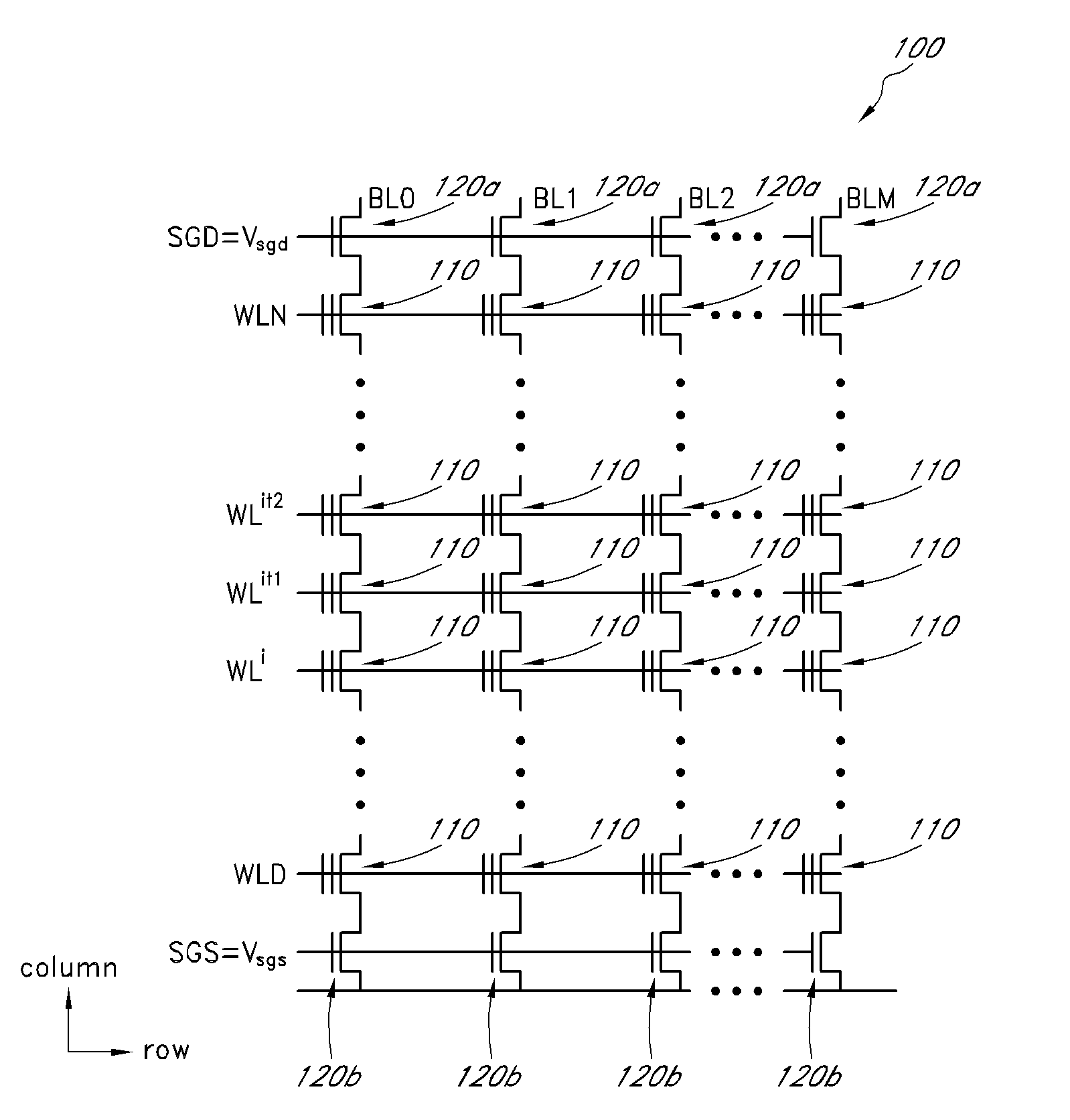
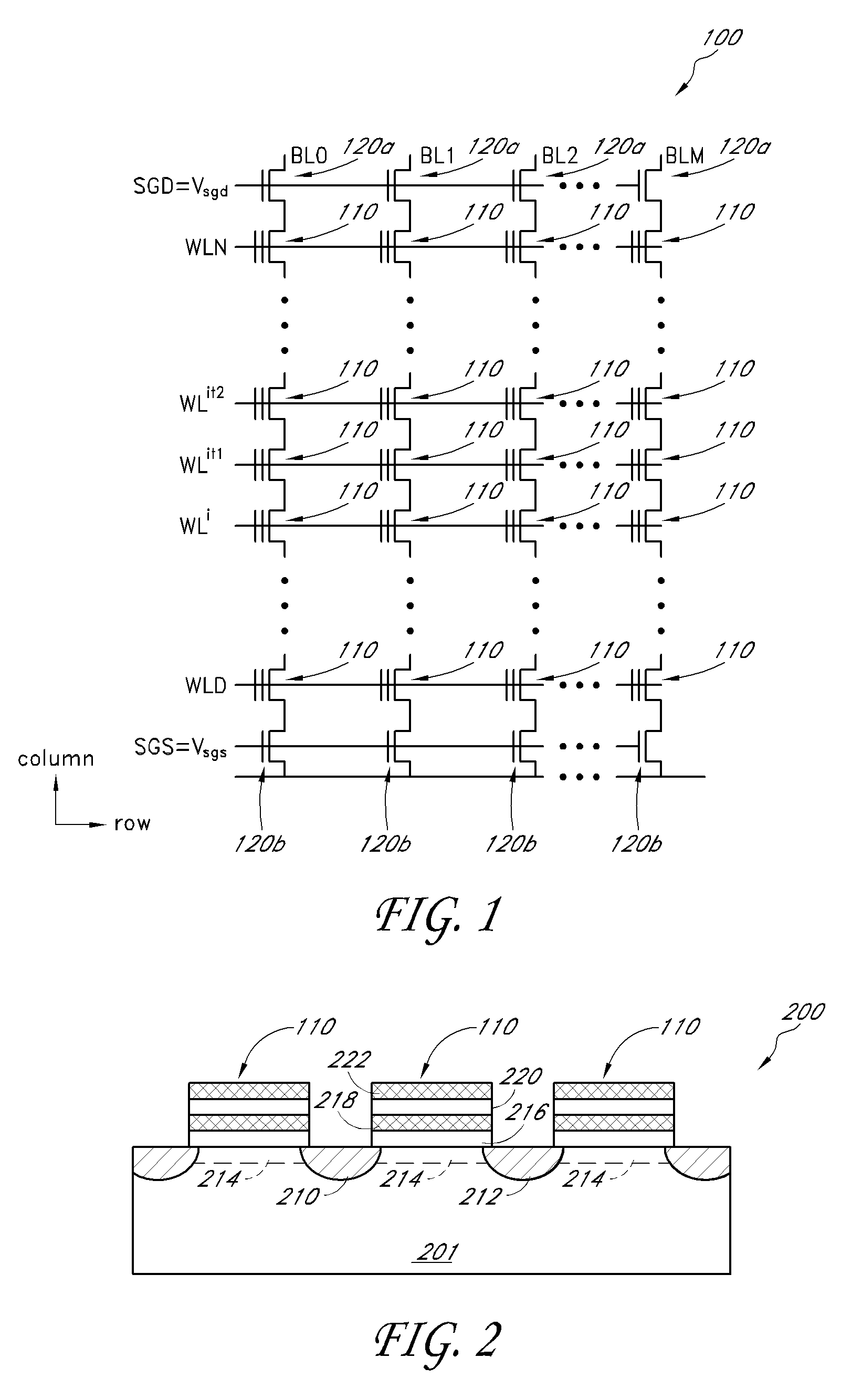
[0018]FIG. 1 illustrates a NAND flash memory array according to one embodiment. The illustrated fl...


PUM


Abstract

Methods and apparatus are disclosed, such as those involving a flash memory device that includes an array of memory cells. One such method includes detecting values of charges stored in selected memory cells in the memory cell array. The method also includes processing the detected values in accordance with a Viterbi algorithm so as to determine data stored in the selected memory cells. In one embodiment, the flash memory cell array includes word lines and bit lines. Detecting the values of charges includes detecting values of charges stored in a selected row of memory cells by selecting one of the word lines. The Viterbi algorithm provides correct data where inter-signal interference between the cells affects the accuracy of read data. For example, the Viterbi algorithm can be used to supplement error correction codes (ECC).

Description

BACKGROUND[0001]1. Field of the Invention[0002]Embodiments of the invention relate to memory devices, and more particularly, in one or more embodiments, to flash memory devices.[0003]2. Description of the Related Art[0004]Flash memory devices are non-volatile memory devices which store information on a semiconductor in a way that needs no power to maintain the information stored therein. Flash memory devices typically include an array of memory cells in a matrix form having columns and rows. Each memory cell includes a charge storage node, such as a floating gate transistor formed on a semiconductor substrate. The cells are arranged to form strings such that the source of the transistor of each cell is coupled to the drain of the transistor of a neighboring cell in each string. The memory cell array includes sense lines (often referred to as bit lines), each of which connects to a column of cells in the memory cell array. The memory cell array also includes select lines (often refer...

Claims


Application Information

Patent Timeline
IPC IPC(8): G11C16/26
CPCG06F11/1068H03M13/23G11C29/04G11C16/26
Inventor ROOHPARVAR, FRANKIESARIN, VISHALRADKE, WILLIAM
Owner MICRON TECH INC
Learn More