
Memory control device

a memory access control and memory technology, applied in the field of memory access control devices, can solve the problems of unfavorable affecting the advantages of the integrated memory architecture, and achieve the effects of avoiding the generation of high peak bandwidth, and reducing the peak bandwidth

Inactive Publication Date: 2009-05-21
PANASONIC CORP
View PDF13 Cites 1 Cited by
  • Summary
  • Abstract
  • Description
  • Claims
  • Application Information

AI Technical Summary

Benefits of technology

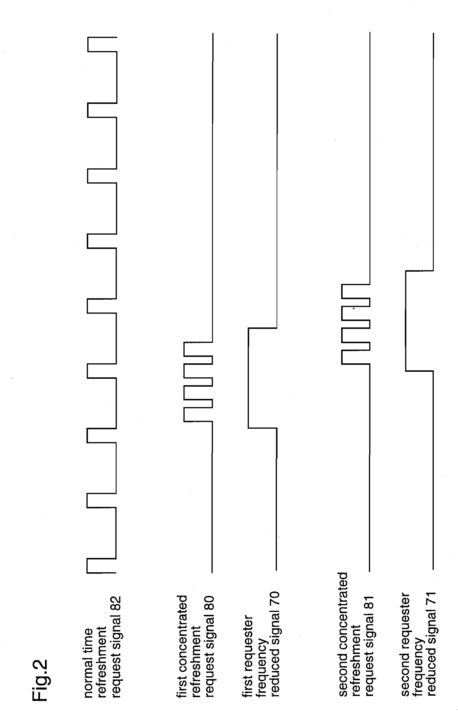
[0016]According to the memory control device according to claim 1 or claim 2, it is possible to appropriately mix the normal time refreshment and the concentrated refreshment, and thereby it is possible to avoid the generation of a high peak bandwidth due to peaks in memory accesses and congestion of refreshments.
[0017]In addition, according to the memory control device according to claim 3, it is possible to provide a memory access control method which is simple and which can realize the normal time refreshment and the concentrated refreshment with a predetermined ratio, in order to reduce the peak bandwidth, being constructed from the information of the bandwidth variation which can be seen a priori.
[0018]In addition, according to the memory control device according to claim 4, it is possible to provide a memory access control method which is simple and which can reduce the peak bandwidth for the refreshments in an information processing apparatus which handles video images.

Problems solved by technology

If the above-mentioned sum of the peak bandwidths is large, countermeasures thereto, such as increasing the memory bath width or raising the operation frequency of the memory, which in turn unfavorably affect the advantages of the integrated memory architecture, are required.

Method used


Image

  • Memory control device
  • Memory control device
  • Memory control device

Examples


first embodiment

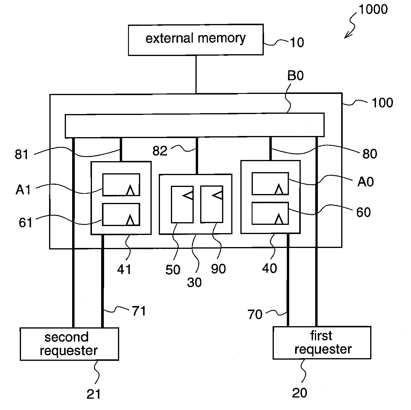
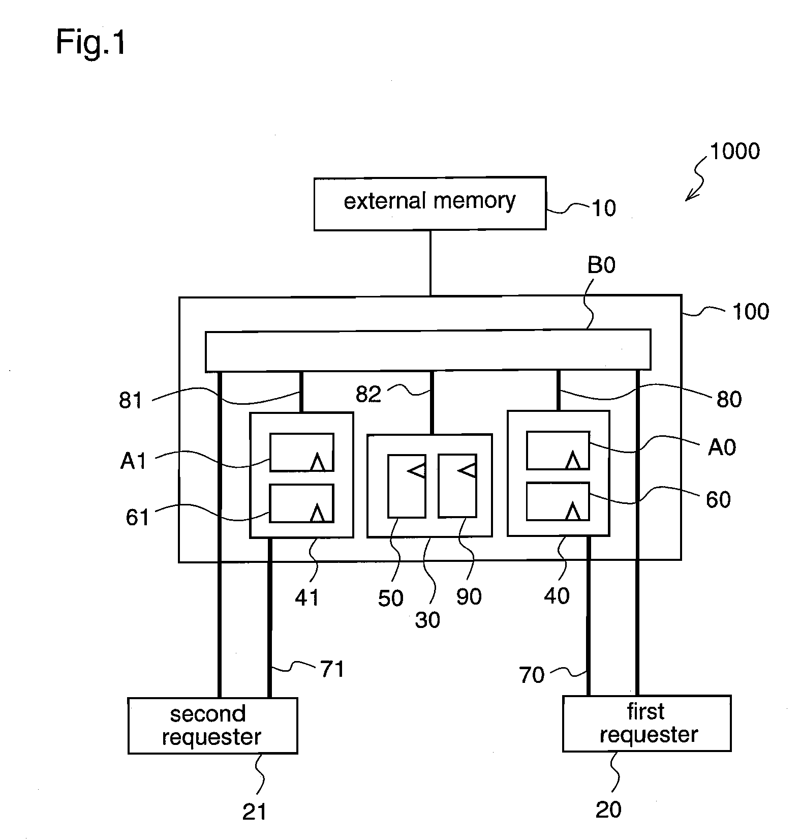
[0043]A memory control device according to a first embodiment of the present invention will be described with reference to FIG. 1.

[0044]FIG. 1 is a diagram illustrating a memory control device 1000 according to a first embodiment of the present invention.

[0045]In the memory control device 1000 shown in FIG. 1, a memory access control circuit 100 is a circuit which controls the accesses from plural requesters to a memory which requires refreshments. This memory control circuit 100 is connected to an external memory 10 which requires refreshments and is also connected to a first requester 20 and a second requester 21 which both issue access requests to the external memory 10.

[0046]In addition, the memory access control circuit 100 includes a normal time refreshment requester 30 which includes therein a normal time frequency register 50 and a normal time refreshment cycle counter 90, a first concentrated refresh requester 40 which includes therein a first concentrated refreshment frequ...


PUM

PropertyMeasurementUnit
timeaaaaaaaaaa
timeaaaaaaaaaa
access frequencyaaaaaaaaaa

Abstract

To provide a memory control circuit in which the bandwidth that is required for the refresh operation is appropriately divided so as to perform smoothing of the peak bandwidth for the memory accesses, and thereby the refresh operations that are required can be accomplished with a low peak bandwidth. A normal time refreshment requester circuit which normally raises a refreshment request for refreshing the memory to the access arbitrator circuit, and a first and second concentrated refreshment requester circuits corresponding to the first and second requesters which in a concentrated manner issues refreshments during while the refreshment request issuing conditions are satisfied such as in a time domain in which the bandwidth for memory accesses are lowered are operated in parallel.

Description

TECHNICAL FIELD[0001]The present invention relates to a memory access control device, and more particularly, to a memory access control circuit for controlling a memory that requires refreshment.BACKGROUND ART[0002]In a system LSI in recent years, integrating two or more functions on a single chip is often carried out. To that end, an integrated memory architecture integrating memories which have been conventionally inherent to individual function blocks respectively is adopted in order to realize a reduced system cost and lowered power consumption.[0003]In the integrated memory architecture, it is required that the sum of the peak bandwidths which are respectively required by the respective function blocks for all the function blocks is within a certain peak bandwidth. If the above-mentioned sum of the peak bandwidths is large, countermeasures thereto, such as increasing the memory bath width or raising the operation frequency of the memory, which in turn unfavorably affect the adv...

Claims


Application Information

Patent Timeline
Patent Type & Authority Applications(United States)
IPC IPC(8): G11B7/085
CPCG06F13/1636G11C2211/4061G11C11/406
Inventor TOMIDA, YASUYUKI
Owner PANASONIC CORP
Learn More