Semiconductor light emitting device, lighting module, lighting apparatus, display element, and manufacturing method for semiconductor light emitting device

a semiconductor light emitting and semiconductor technology, applied in semiconductor devices for light sources, discharge tubes, lighting and heating apparatus, etc., can solve the problems of insufficient light reflection on the wall of the reflective hole, inability to achieve desired light collection efficiency, and inability to produce small amounts of light. to achieve the effect of efficient collection

Active Publication Date: 2009-05-28
SATCO PRODS
View PDF7 Cites 41 Cited by
  • Summary
  • Abstract
  • Description
  • Claims
  • Application Information

AI Technical Summary

Benefits of technology

[0019]The object can be also achieved by a lighting module or a lighting apparatus which includes the above-described semiconductor light emitting device on a mounting substrate. Here, a printed wiring board with a reflective film can be used as the mounting substrate. Therefore, light emitted from the semiconductor light emitting device can be efficiently collected to be irradiated toward an object.

Problems solved by technology

Here, although such a current white LED has higher luminance than previous ones, a single LED bare chip can only produce a small amount of light.
This means that the wall of the reflective hole does not appropriately reflect light emitted from a side surface of the LED bare chip forward.
Accordingly, a desired light collection efficiency can not be achieved.
However, the technique is difficult to be used for mounting a white LED on a printed wiring board with a reflective film.
Firstly, it is difficult to form an adhesive layer adhering a reflective board to a printed wiring board, at an even thickness.
Therefore, a relative location of each reflective hole provided in the reflective board with respect to a corresponding white LED in a direction of light emission is not uniform.
Accordingly, a light collection efficiency of each reflective hole is not uniform.
Secondly, a predetermined relative location between a reflective hole and a bare chip (a white LED chip) is not likely to be achieved.
This is because a bare chip is not precisely mounted on a designed location on a printed wiring board, and a reflective board can not be perfectly aligned with the printed wiring board.
This degrades a light collection efficiency.
Thirdly, when a printed wiring board with a reflective board is utilized, an additional step is required for adhering the reflective board which has been separately manufactured to the printed wiring board.
These problems are not created if a printed wiring board with a reflective film, which has a reflective hole formed as part of the printed wiring board, is utilized.

Method used


Image

  • Semiconductor light emitting device, lighting module, lighting apparatus, display element, and manufacturing method for semiconductor light emitting device
  • Semiconductor light emitting device, lighting module, lighting apparatus, display element, and manufacturing method for semiconductor light emitting device
  • Semiconductor light emitting device, lighting module, lighting apparatus, display element, and manufacturing method for semiconductor light emitting device

Examples


first embodiment

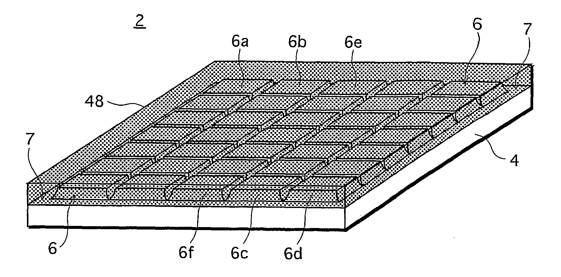
[0051]FIG. 3A is an external perspective view illustrating a construction of a white LED array chip 2 which is one type of a semiconductor light emitting device (hereinafter simply referred to as an LED array chip 2). FIG. 3B is a plan view illustrating the LED array chip 2. FIG. 3A is mainly intended to show how LEDs 6 (described later) are arranged, and therefore does not show minute depressions and protrusions on surfaces of the LEDs 6. FIG. 3B does not show a phosphor film 48 (described later). It should be noted that a reduced scale for each constituent is not uniform in any of the drawings including FIGS. 3A and 3B.

[0052]As shown in FIGS. 3A and 3B, the LED array chip 2 is formed in such a manner that the LEDs 6 are arranged in a matrix of N rows and M columns (in the first embodiment, a matrix of seven rows and five columns, in total 35 LEDs 6) on a non-doped (highly resistant) SiC substrate 4 which is a semiconductor substrate (hereinafter simply referred to as an SiC substr...

second embodiment

[0086]FIG. 10 is an external perspective view illustrating a construction of an LED array chip 302 relating to a second embodiment, which is one type of a semiconductor light emitting device.

[0087]The LED array chip 302 relating to the second embodiment basically has the same construction as the LED array chip 2 relating to the first embodiment (shown in FIGS. 3 to 5), except for a configuration of an uneven light extraction surface of each LED to enhance a light extraction efficiency, and a configuration of an SiC substrate. Common constituents of the LED array chip 302 are identified by the same reference numbers as in the first embodiment. The following description includes a brief or no mention of those common constituents, and mainly focuses on the different configurations between the LED array chips 2 and 302.

[0088]As shown in FIG. 10, a non-doped (highly resistant) SiC substrate 304 which constitutes the LED array chip 302 (hereinafter simply referred to as an SiC substrate 3...

third embodiment

[0109]According to the first and second embodiments, the anode electrode (34 and 334) and the cathode electrode (32) of the LED array chip (2 and 302) are electrically connected to the power supply terminals (36 and 38, 336 and 338) on the back surface of the SiC substrate (4 and 304) by conductive members including the plated-through holes (42 and 46, 342 and 346) provided in the SiC substrate (4 and 304). According to a third embodiment, however, such conductive members include conductive films formed on side surfaces of an SiC substrate, instead of the plated-through holes (42 and 46, 342 and 346). An LED array chip 402 relating to the third embodiment basically has the same construction as the LED array chip 302 relating to the second embodiment, except for that conductive films are provided instead of the plated-through holes (42 and 46, 342 and 346) and that the removed portions 304a and 304b are not created. Common constituents of the LED array chip 402 are identified by the ...


PUM


Abstract

In an LED array chip (2), LEDs (6) are connected together in series by a bridging wire (30). The LEDs (6) each have a semiconductor multilayer structure (8-18) including a light emitting layer (14). Here, the semiconductor multilayer structure (8-18) is epitaxially grown on a front surface of an SiC substrate (4). A phosphor film (48) covers the LEDs (6). Two power supply terminals (36 and 38), which are electrically independent from each other, are formed on a back surface of the SiC substrate (4). The power supply terminal (36) is connected to a cathode electrode (32) of an LED (6a) at a lower potential end by a bridging wire (40) and a plated-through hole (42). The power supply terminal (38) is connected to an anode electrode (34) of an LED (6d) at a higher potential end by a bridging wire (44) and a plated-through hole (46).

Description

RELATED APPLICATIONS[0001]The present application is a divisional application from U.S. patent application Ser. No. 10 / 580,929 filed May 30, 2006.TECHNICAL FIELD[0002]The present invention relates to a semiconductor light emitting device such as a light emitting diode (LED) chip, a manufacturing method for the semiconductor light emitting device, and a lighting module, a lighting apparatus, and a display element using the semiconductor light emitting device. The present invention especially relates to a semiconductor light emitting device which includes a phosphor to produce visible light of a desired color.BACKGROUND ART[0003]In the field of LEDs, vigorous researches are recently conducted to use white LEDs for lighting, in accordance with development of white LEDs with higher luminance. Having a feature of a point light source, LEDs are expected to replace halogen lamps and the like which have been conventionally used as spotlighting in a shop, a museum, a showroom, and the like.[...

Claims


Application Information

Patent Timeline
Patent Type & Authority Applications(United States)
IPC IPC(8): H01L33/00H01L27/15H01J1/62H01L51/52H01L51/56H01L33/06F21K99/00H01L25/075H01L33/08H01L33/10H01L33/32H01L33/34H01L33/38H01L33/42H01L33/50H01L33/56H01L33/58H01L33/60
CPCF21K9/00H01L25/0753H01L2924/0002H01L33/50H01L2924/00
Inventor NAGAI, HIDEO
Owner SATCO PRODS
Why Eureka
Try Eureka