

Jitter generator for generating jittered clock signal
a clock signal and generator technology, applied in the field of jitter generators, can solve the problems of increasing the bit error rate (ber) of the receiver, the test instrument is expensive, and is not suitable for mass production testing, so as to save the cost of the test instrumen
- Summary
- Abstract
- Description
- Claims
- Application Information
AI Technical Summary
Benefits of technology
Problems solved by technology
Method used
Image

Examples
first embodiment
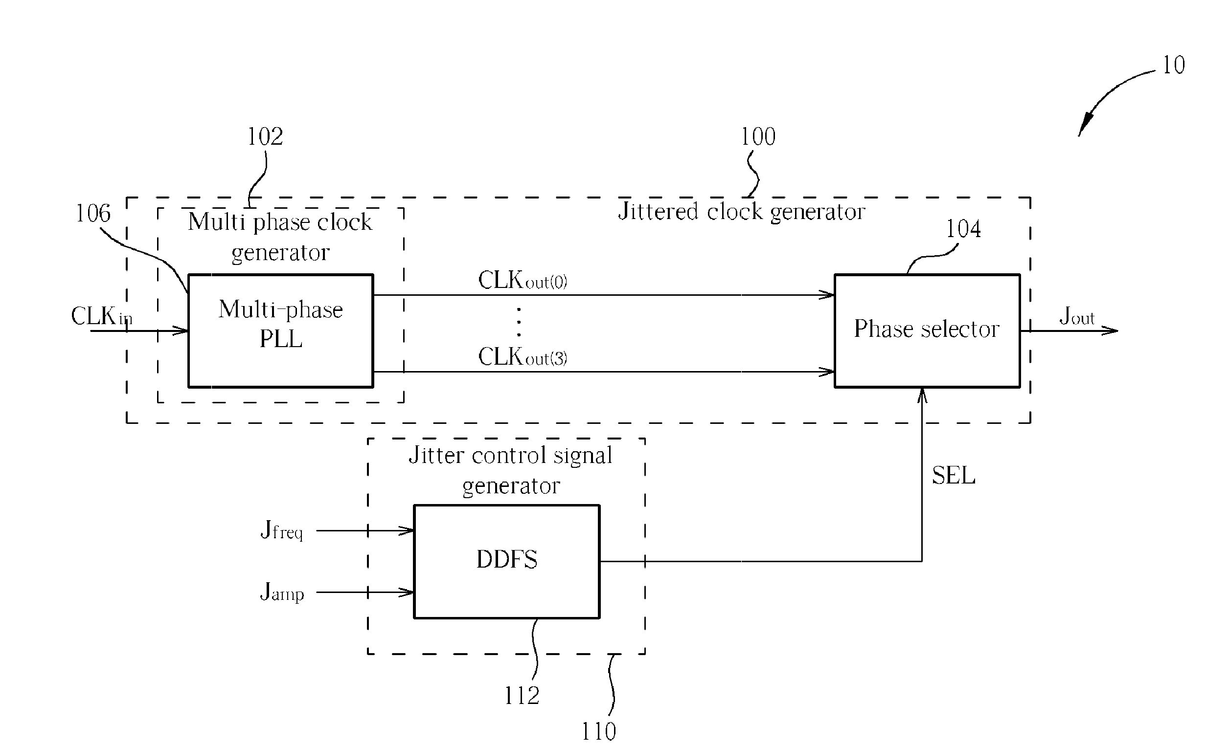
[0021]Please refer to FIG. 1. FIG. 1 is a block diagram of a jitter generator 10 according to the present invention. The jitter generator 10 includes a jittered clock generator 100 and a jitter control signal generator 110, and the jittered clock generator 100 comprises a multi-phase clock generator 102 and a phase selector 104. The jitter control signal generator 110 is utilized for selecting at least a set of digital control codes from a plurality of candidate digital control codes at individual time points and respectively outputting a plurality of selected digital control codes. In this embodiment, the jitter control signal generator 110 is implemented with a direct digital frequency synthesizer (DDFS) 112. The DDFS 112 is a component for generating digitalized arbitrary waveforms, where the operation thereof is well known in the art and therefore not explained in detail here. According to the jitter frequency control signal Jfreq and the jitter amplitude control signal Jamp the...
second embodiment
[0022]Please refer to FIG. 5. FIG. 5 is a block diagram of a jitter generator 20 according to the present invention. The jitter generator 20 includes a jittered clock generator 200 and a jitter control signal generator 210, where the jittered clock generator 200 includes a multi-phase clock generator 202 and a phase selector 204, and the jitter control signal generator 210 includes a DDFS 212 and a decoder 214. The architecture of the circuit in FIG. 5 is almost the same as FIG. 1, where the only difference is that the jitter control signal generator 210 includes a decoder 214, where the decoder 214 is utilized for decoding and converting the digital wave signal outputted from the DDFS 212 into the digital control code SEL.
[0023]Please note that, the aforementioned implementation of the jitter control signal generators respectively disclosed in the first embodiment and the second embodiment is for illustrative purposes only and not a limitation of the present invention. Therefore, s...
third embodiment
[0024]Please refer to FIG. 6, FIG. 6 is a block diagram of a jitter generator 30 according to the present invention. The jitter generator 30 includes a jitter control signal generator 320 for generating a jitter control signal Jctl and a jittered clock generator 300 for generating the jittered clock signal Jout according to the jitter control signal Jctl. In this embodiment, the jitter control signal generator 320 includes a DDFS 322 and a digital-to-analog converter (DAC) 324. The DDFS 322 can be controlled to synthesize the digital wave signal needed according to the jitter frequency control signal Jfreq and the jitter amplitude control signal Jamp, and the DAC 324 converts the digital wave signal to output a jitter control signal Jctl having continuous waveforms, that is, the jitter control signal Jctl is an analog signal.
[0025]In this embodiment, the jittered clock generator 300 is implemented with the phase interpolated delay locked loop (PI DLL) 400. Please refer to FIG. 7. FI...
PUM
 Abstract
Description
Claims
Application Information