Display apparatus

a display apparatus and display technology, applied in the field of display apparatuses, can solve the problems of display unevenness in response to image patterns, inability to keep the emission light luminance fixed, and complicated configuration of pixel circuits, so as to achieve the effect of reducing the number of wiring lines, reducing the size of the pixel array section, and improving the definition of the display apparatus

Active Publication Date: 2009-05-28
SONY CORP
View PDF4 Cites 44 Cited by
  • Summary
  • Abstract
  • Description
  • Claims
  • Application Information

AI Technical Summary

Benefits of technology

[0053]As a result, only it is necessary to apply some modification to the driving timings and so forth of the transistors on the basis of the 2 TR driving configuration, and the number of components of the pixel circuit and the number of wiring lines can be reduced significantly and the pixel array section can be reduced in size. Consequently, a higher definition of the display apparatus can be achieved readily. Further, while simplification of the

Problems solved by technology

As a result, even if a function for keeping the driving signal fixed is applied by threshold value correction, mobility correction or bootstrap operation, the driving signal such as driving current is fluctuated by potential fluctuation by the leak current, resulting in failure to keep the emission light luminance fixed.
If the level of this phenomenon differs among different pixels, then the display image becomes rough or uneven, and where the leak current amount is influenced by the image pattern, display unevenness appears in

Method used


Image

  • Display apparatus
  • Display apparatus
  • Display apparatus

Examples


Embodiment Construction

[0082]Hereinafter, an embodiment of the present invention will be described with reference to the accompanying drawings.

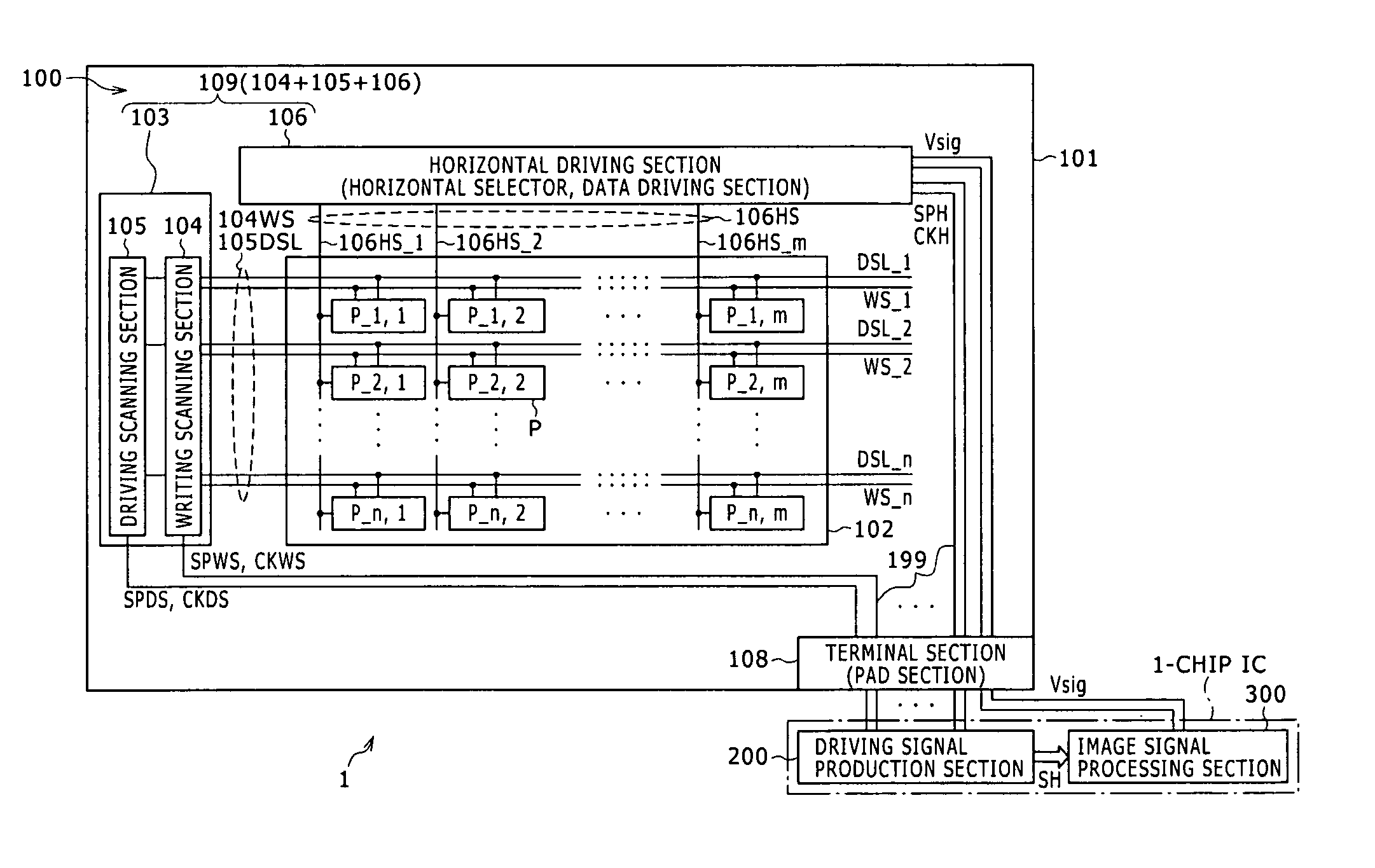
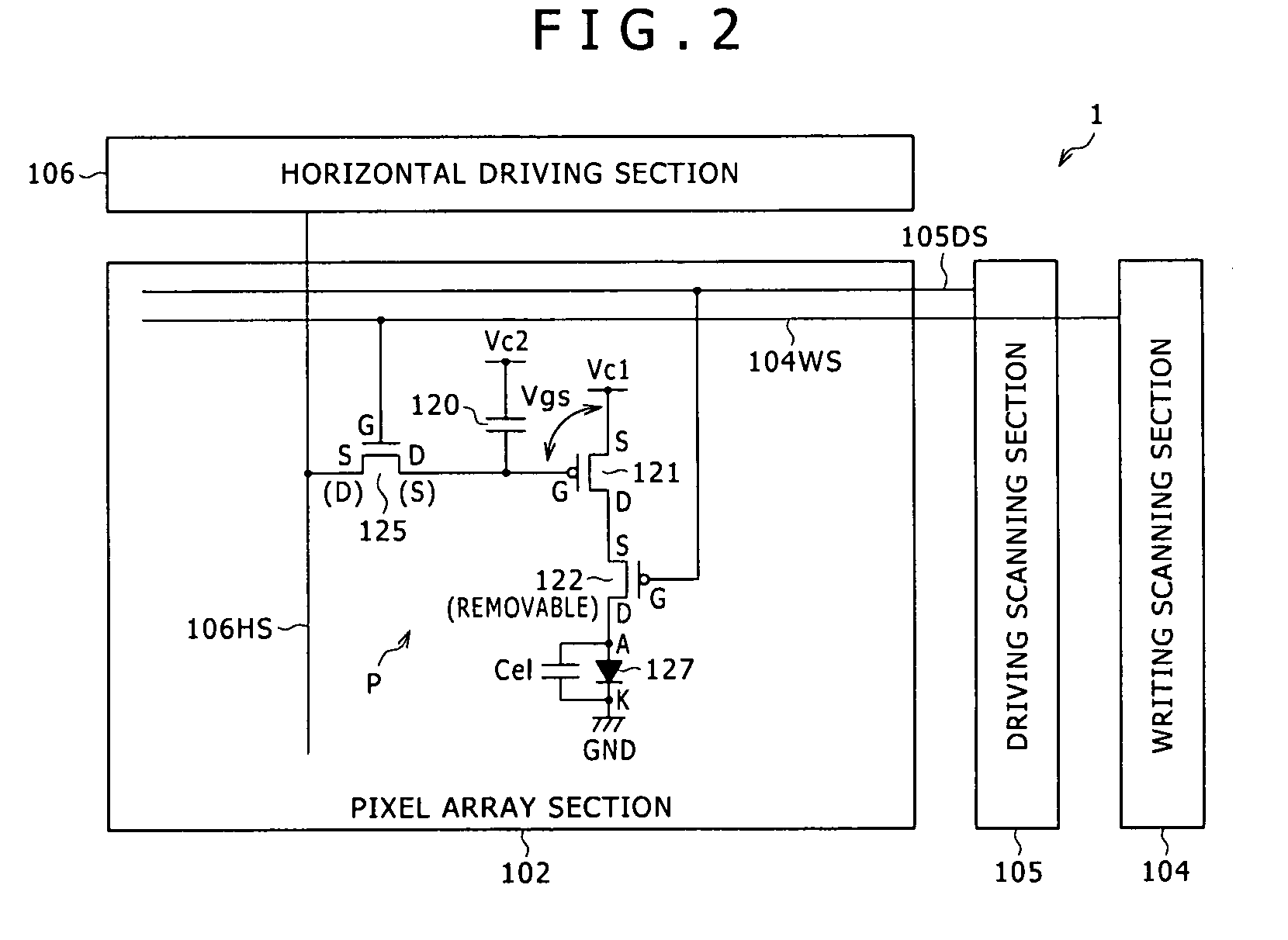
[0083]Referring first to FIG. 1, there are shown different examples of a configuration of an active matrix type display apparatus as a display apparatus according to a preferred embodiment of the present invention. In the present embodiment, the present invention is applied to an active matrix type organic EL display apparatus (hereinafter referred to simply as “organic EL display apparatus”) wherein, for example, an organic EL element and a polysilicon thin film transistor (TFT) are used as a display element (electro-optical element or light emitting element) and an active element of each pixel, respectively. Further, in the organic EL display apparatus, such organic EL elements are formed on a semiconductor substrate on which such thin film transistors are formed.

[0084]It is to be noted that, while an organic EL element is described below particularly as an examp...


PUM


Abstract

Disclosed herein is a display apparatus, including: a pixel array section including a plurality of pixel circuits disposed in a matrix and each including a driving transistor for producing driving current, a storage capacitor for storing information of a image signal amplitude, an electro-optical element connected to an output terminal side of the driving transistor, and a sampling transistor for writing information of the signal amplitude into the storage capacitor, the driving transistor being operable to produce driving current based on the information stored in the storage capacitor and supply the driving current to the electro-optical element to cause the electro-optical element to emit light; a driving signal fixing circuit for keeping the driving current fixed; and a light blocking layer provided on the light input side of a transistor which participates in the driving signal fixing function and for preventing appearance of leak current of the transistors arising from light irradiation.

Description

CROSS REFERENCES TO RELATED APPLICATIONS[0001]The present invention contains subject matter related to Japanese Patent Application JP 2007-307862, filed in the Japan Patent Office on Nov. 28, 2007, the entire contents of which being incorporated herein by reference.BACKGROUND OF THE INVENTION[0002]1. Field of the Invention[0003]This invention relates to a display apparatus which includes a pixel array section including a plurality of pixel circuits (hereinafter referred to also as pixels) disposed in rows and columns and each including an electro-optical element (hereinafter referred to as display element or light emitting element). More particularly, the present invention relates to a display apparatus of the active matrix type wherein a plurality of pixel circuits each including an electro-optical element whose emission light luminance varies depending upon current flowing therethrough are disposed in rows and columns and display driving in a unit of a pixel is carried out by an a...

Claims


Application Information

Patent Timeline
IPC IPC(8): G09G3/30
CPCG09G3/3233G09G2300/0819G09G2300/0842G09G2300/0861G09G2300/0866H01L27/3272G09G2320/0233G09G2320/0238G09G2320/043G09G2320/045G09G2310/0256H10K59/126
Inventor YAMAMOTO, TETSUROUCHINO, KATSUHIDE
Owner SONY CORP
Why Eureka
Try Eureka