Plasma display device and plasma-display-panel driving method

a technology of plasma display device and plasma display panel, which is applied in the direction of instruments, television systems, computing, etc., can solve the problems of unstable address discharge, deterioration of image display quality, and unstable narrow erasing discharg

Inactive Publication Date: 2009-05-28
PANASONIC CORP
View PDF22 Cites 5 Cited by
  • Summary
  • Abstract
  • Description
  • Claims
  • Application Information

AI Technical Summary

Benefits of technology

[0014]According to this configuration, it is possible to generate a stable address discharge in a high-brightness panel, wi...

Problems solved by technology

However, with an increase in screen size or an increase in brightness of a panel, the narrow erasing discharge tends to get unstable.
Accordingly, the address discharge gets unstable and there are thus problems in that the address discharge may not be generated in the discharged cells to perform a display to deteriorate image display quality or that a voltage for generating the address discharge may be raised.
When a voltage applied to the discharge cells is raised to stably generate the discharge, a so-called crosstalk that a di...

Method used


Image

  • Plasma display device and plasma-display-panel driving method
  • Plasma display device and plasma-display-panel driving method
  • Plasma display device and plasma-display-panel driving method

Examples


first embodiment

[0070]Hereinafter, a plasma display device according to a first embodiment of the invention will be described with reference to the drawings.

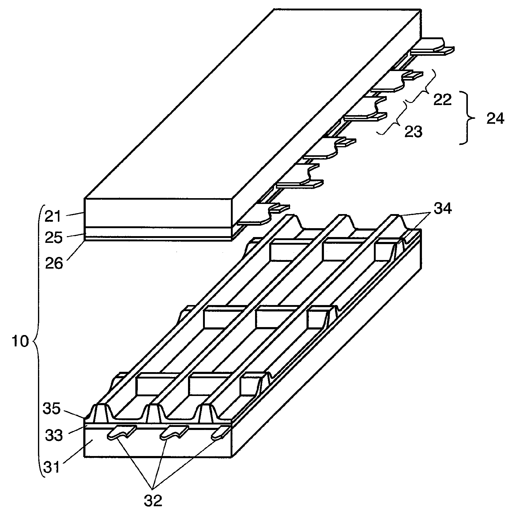
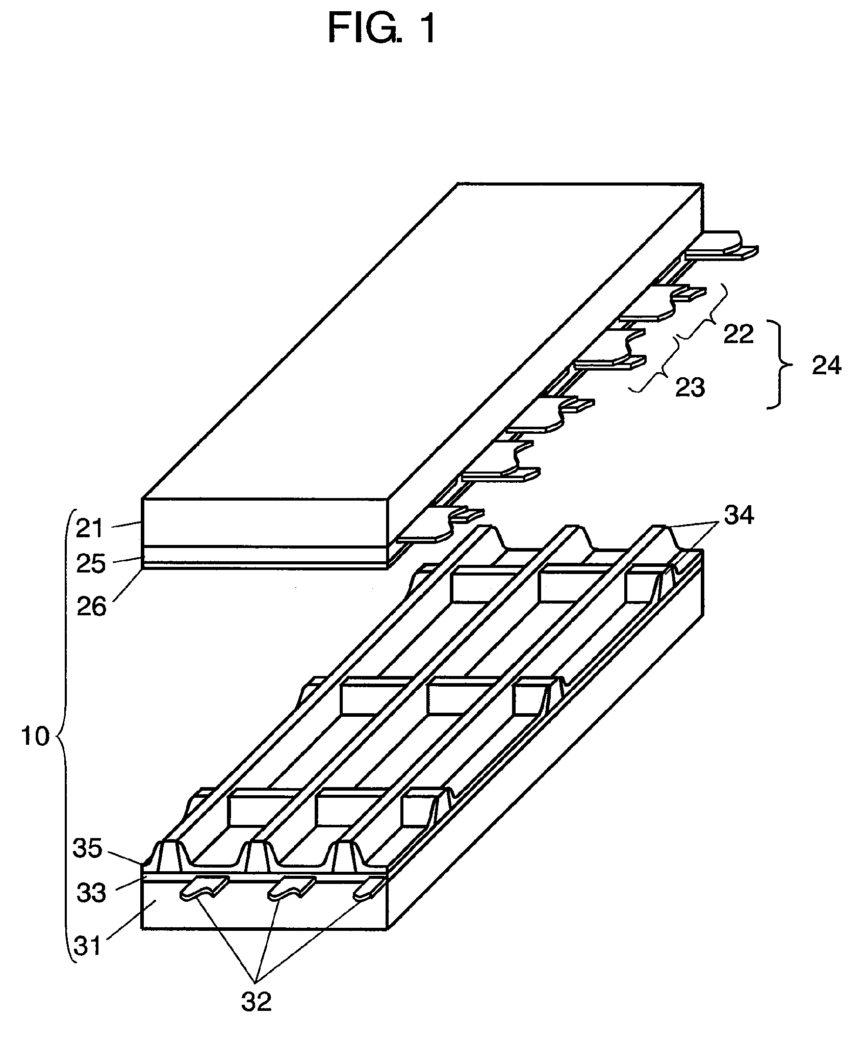
[0071]FIG. 1 is an exploded perspective view illustrating a structure of panel 10 according to a first embodiment of the invention. Plural display electrode pairs 24 each having scan electrode 22 and sustain electrode 23 are formed on front glass substrate 21. Dielectric layer 25 is formed to cover scan electrodes 22 and sustain electrodes 23 and protective layer 26 is formed on dielectric layer 25.

[0072]In order to lower a breakdown start voltage in discharge cell), protective layer 26 is formed of a material containing as a major component MgO which has been used as a material of a panel and which has a high secondary electron emission coefficient and an excellent durability when neon (Ne) and xenon (Xe) gases enclosed therein.

[0073]Plural data electrodes 32 are formed on rear substrate 31. Dielectric layer 33 is formed to cover data electrod...

second embodiment

[0155]Next, a plasma display device according to a second embodiment of the invention will be described with reference to the drawings.

[0156]FIG. 1 is an exploded perspective view illustrating a part of panel 10 according to the second embodiment of the invention. Plural display electrode pairs 24 each having scan electrode 22 and sustain electrode 23 are formed on front glass substrate 21. Dielectric layer 25 is formed to cover scan electrodes 22 and sustain electrodes 23 and protective layer 26 is formed on dielectric layer 25.

[0157]In order to lower a breakdown start voltage in discharge cells, protective layer 26 is formed of a material containing as a major component MgO which has been used as a material of a panel and which has a high secondary electron emission coefficient and an excellent durability when neon (Ne) and xenon (Xe) gases enclosed therein.

[0158]Plural data electrodes 32 are formed on rear substrate 31. Dielectric layer 33 is formed to cover data electrodes 32 an...


PUM


Abstract

In a plasma-display-panel driving method, a field period is divided into a plurality of sub fields, each of which has an address period for allowing discharge cells to selectively generate an address discharge and a sustain period for allowing the discharge cells having generated the address discharge to generate a sustain discharge by a number of times corresponding to a brightness weight. In the sustain period, a period for setting display electrode pairs to the base potential is disposed between the sustain pulse for causing the final sustain discharge in the sustain period and the previous sustain pulse. In a time interval corresponding to the lighting ratio of the discharge cells in the sub field after applying to the display electrode pairs a voltage for generating the final sustain discharge, a voltage for reducing the potential difference between electrodes of the display electrode pairs is applied to the display electrode pairs. Accordingly, it is possible to generate a stable address discharge and thus to reduce a crosstalk without increasing the voltage for generating the address discharge.

Description

TECHNICAL FIELD[0001]The present invention relates to a plasma display device used in a wall-mounted television or a large-scaled monitor and a plasma-display-panel driving method.BACKGROUND ART[0002]In an AC surface discharge panel representative of a plasma display panel (hereinafter, simply referred to as “panel”), plural discharge cells are formed between a front substrate and a rear substrate opposed to each other. In the front substrate, plural display electrode pairs each including a scan electrode and a sustain electrode are on a front glass substrate to be parallel to each other and a dielectric layer and a protective layer are formed to cover the display electrode pairs. In the rear substrate, plural parallel data electrodes are formed on a rear glass substrate, a dielectric layer is formed to cover the data electrode, plural barrier ribs are formed thereon to be parallel to the data electrodes, and a phosphor layer is formed on the surface of the dielectric layer and on t...

Claims


Application Information

Patent Timeline
IPC IPC(8): G09G5/00G09G3/28G09G3/288G09G3/291G09G3/292G09G3/294G09G3/296G09G3/298
CPCG09G3/2022G09G3/2927G09G3/2965H04N5/70G09G2320/048G09G2360/16G09G2310/066G09G3/296G09G3/294
Inventor SHOJI, HIDEHIKOORIGUCHI, TAKAHIKOUEDA, MITSUO
Owner PANASONIC CORP
Why Eureka
Try Eureka