Epitaxial Wafer for Semiconductor Light Emitting Diode and Semiconductor Light Emitting Diode Using Same

a light-emitting diode and semiconductor technology, applied in semiconductor devices, lasers, semiconductor lasers, etc., can solve the problems of deterioration of light-emitting characteristics in the active layer, affecting the operation reducing the lifetime of the semiconductor light-emitting device, so as to achieve high-reliability, stable high-output operation

Inactive Publication Date: 2009-06-04
SUMITOMO CHEM CO LTD
View PDF6 Cites 10 Cited by
  • Summary
  • Abstract
  • Description
  • Claims
  • Application Information

AI Technical Summary

Benefits of technology

[0023]According to the present invention, it is possible to provide an epitaxial wafer for a semiconductor light emitting device in which diffusion of an appropriate (optimum) amount of Zn into the Mg-doped p-type cladding layer and active layer is occurred during the

Problems solved by technology

As a result, the full width of half maximum of the photoluminescence spectrum in the active layer becomes large, causing critical problems such as deterioration in light emitting characteristics in the active layer and reduction in lifetime.
Acco

Method used


Image

  • Epitaxial Wafer for Semiconductor Light Emitting Diode and Semiconductor Light Emitting Diode Using Same
  • Epitaxial Wafer for Semiconductor Light Emitting Diode and Semiconductor Light Emitting Diode Using Same
  • Epitaxial Wafer for Semiconductor Light Emitting Diode and Semiconductor Light Emitting Diode Using Same

Examples


example 1

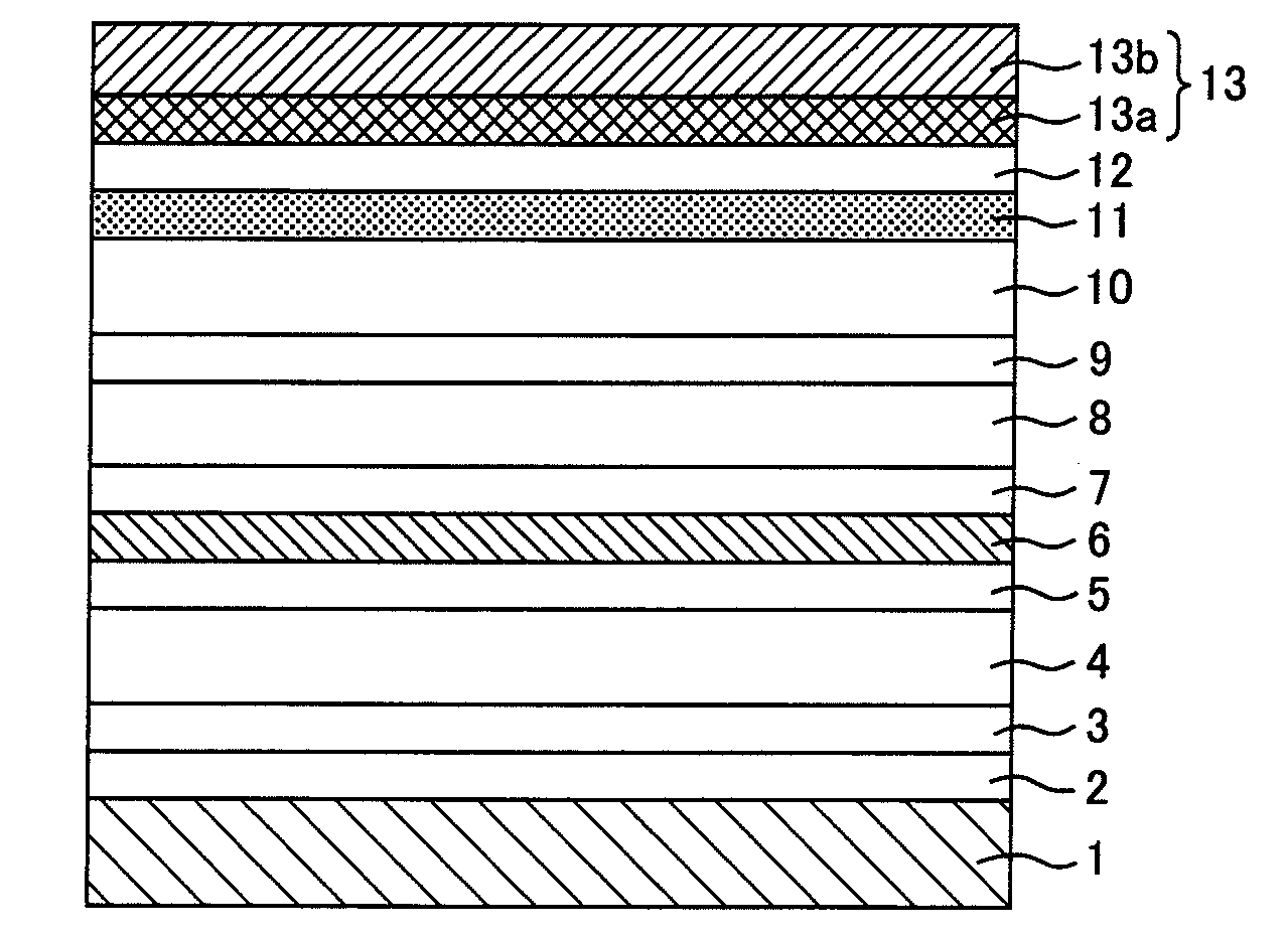
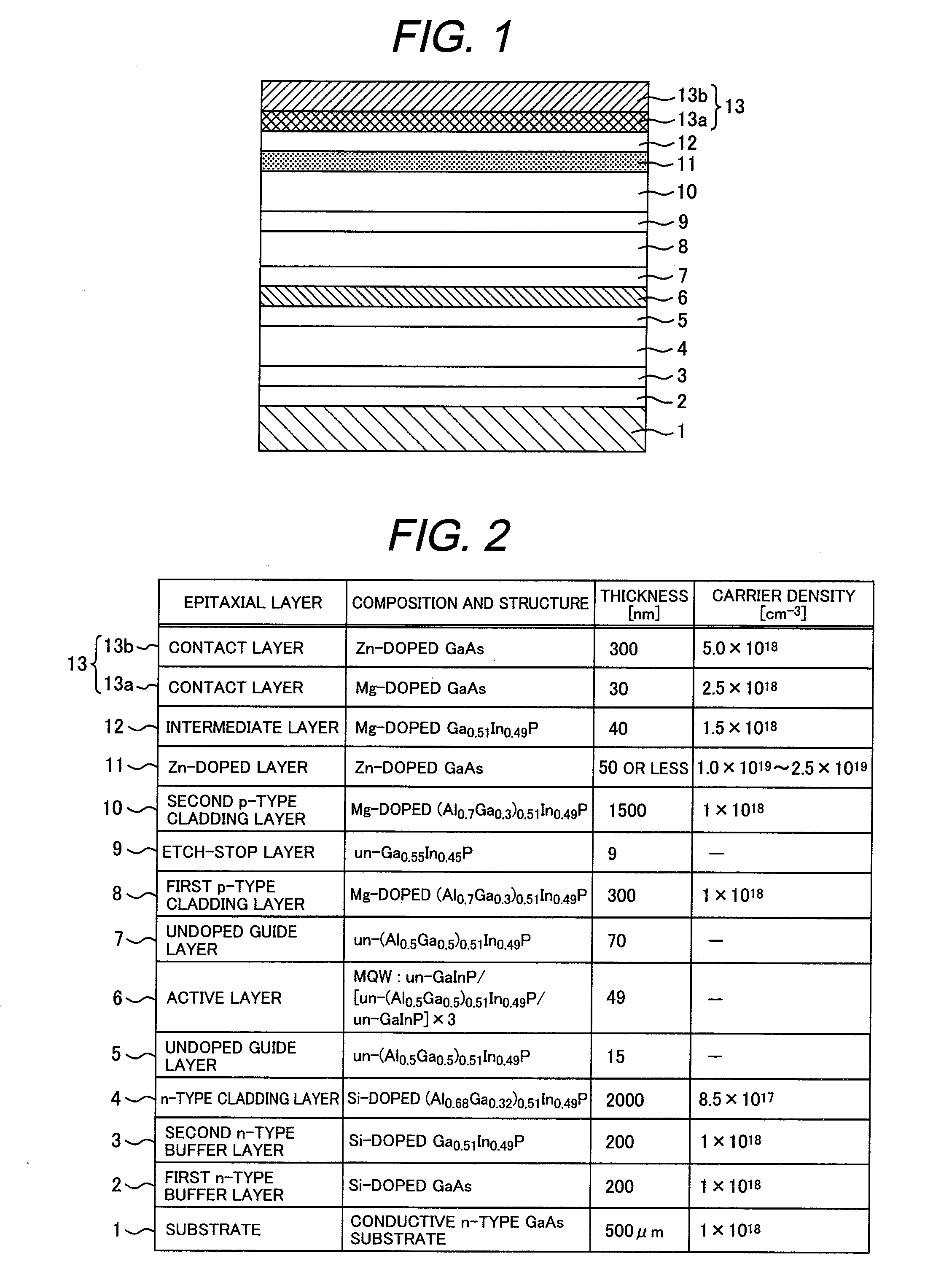
[0039]An epitaxial wafer for a semiconductor light emitting device (semiconductor laser) in Example 1 has the same cross sectional structure as in the above embodiment shown in FIG. 1. Detail specifications, e.g., composition, structure, thickness, and carrier density of each epitaxial layer are shown in FIG. 2. FIG. 2 is a table indicating a structure of an epitaxial wafer for a semiconductor light emitting device in Example 1 of the present invention. The symbol “un-” in FIG. 2 represents “undoped”.

[0040]As shown in FIG. 2, the epitaxial wafer for a semiconductor light emitting device in Example 1 has, on an n-type GaAs substrate 1 made of GaAs: a first buffer layer 2 made of GaAs; a second buffer layer 3 made of Ga0.51In0.49P; an n-type cladding layer 4 made of (Al0.68Ga0.32)0.51In0.49P; an undoped guide layer 5 made of (Al0.50Ga0.50)0.51In0.49P; an active layer 6 having a multiple quantum well (MQW) structure; an undoped guide layer 7 made of (Al0.50Ga0.50)0.51In0.49P; a first p...

example 2

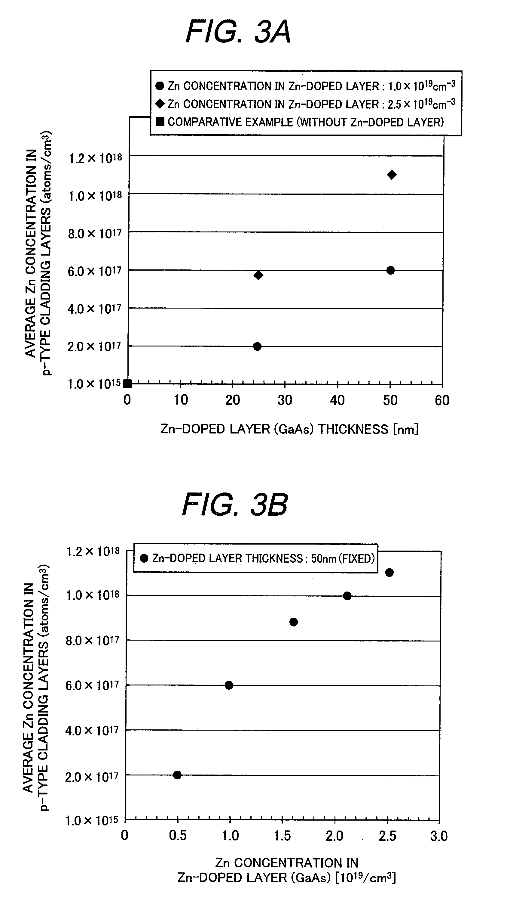
[0046]Example 2 differs from Example 1 in that after the second p-type cladding layer 10 made of AlGaInP was grown, Zn planer doping was carried out to form the Zn planer-doped layer, instead of stacking the Zn-doped layer 11 made of GaAs on the second p-type cladding layer 10 as in Example 1. The other aspects were the same as in Example 1.

[0047]In Example 2, the Zn flow rate during planer doping and a time of the planer doping were changed to investigate the influence to the amount of Zn which diffused into the second p-type cladding layer 10. Experimental results are shown in FIGS. 4A and 4B. FIG. 4A is a graph showing a relationship between average Zn concentration in the p-type cladding layers and the planer doping time during the growth in Example 2 of the present invention; FIG. 4B is a graph showing a relationship between average Zn concentration in the p-type cladding layers and the Zn flow rate during the planer doping in Example 2 of the present invention. As mentioned ab...


PUM


Abstract

An epitaxial wafer for a semiconductor light emitting device according to the present invention in which at least an n-type cladding layer formed with a mixed crystal made of an AlGaInP material, an active layer, a p-type Mg-doped cladding layer, and a p-type contact layer are stacked successively in that order on an n-type GaAs substrate, and the p-type contact layer is formed as at least two layers that are an Mg-doped contact layer and a Zn-doped contact layer stacked thereon when viewed from the n-type GaAs substrate, comprises a Zn-doped layer which is inserted between the p-type Mg-doped cladding layer and the p-type contact layer.

Description

CLAIM OF PRIORITY[0001]The present application claims priority from Japanese patent application serial no. 2007-309650 filed on Nov. 30, 2007, the content of which is hereby incorporated by reference into this application.BACKGROUND OF THE INVENTION[0002]1. Field of the Invention[0003]The present invention relates to an epitaxial wafer used in a semiconductor light emitting device such as a light emitting diode or semiconductor laser as well as to a semiconductor light emitting device fabricated by using the epitaxial wafer.[0004]2. Description of Related Art[0005]The metal organic vapor phase epitaxy (MOVPE) method has been mainly used as a growth method of a crystal used in a semiconductor light emitting device. When a semiconductor crystal including compounds in the III and V groups is grown in this method, a substrate disposed in a vapor phase epitaxy apparatus is heated, after which a III-group metal organic raw gas, V-group raw gas, carrier gas, and dopant raw gas, which are u...

Claims


Application Information

Patent Timeline
IPC IPC(8): H01L33/00H01L29/20H01L33/14H01L33/30
CPCB82Y20/00H01L33/14H01L33/305H01S5/34326H01S5/3054H01S5/3063H01S5/3072H01S5/0421
Inventor TAKEUCHI, TAKASHISUKEGAWA, TOSHIMITSU
Owner SUMITOMO CHEM CO LTD
Why Eureka
Try Eureka