Electronic part and method of producing the same

Inactive Publication Date: 2009-06-04
PANASONIC CORP
View PDF6 Cites 10 Cited by
  • Summary
  • Abstract
  • Description
  • Claims
  • Application Information

AI Technical Summary

Benefits of technology

[0020]According to this configuration, an accurate gap can be formed betwe

Problems solved by technology

In addition, since the processes for forming the bonding layer 23 and gap-set

Method used


Image

  • Electronic part and method of producing the same
  • Electronic part and method of producing the same
  • Electronic part and method of producing the same

Examples


first embodiment

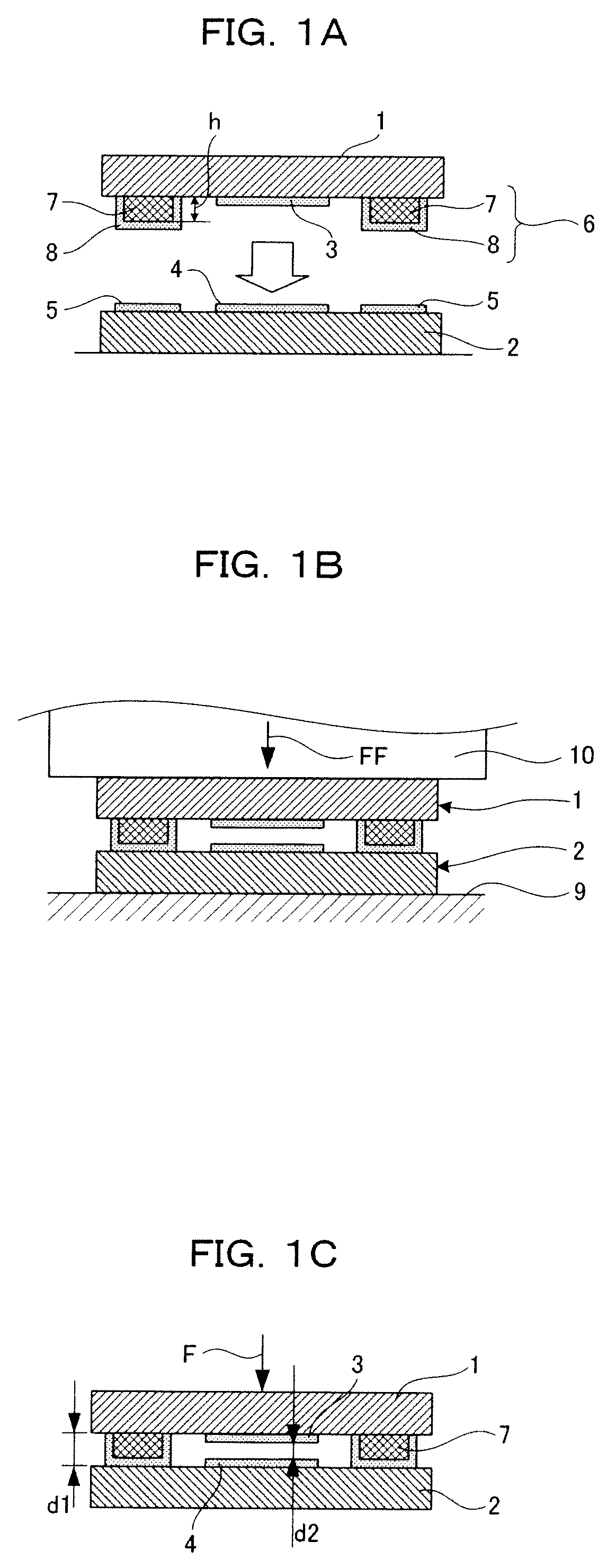
[0043]FIGS. 1A to 1C and FIG. 2 show a first embodiment of the present invention.

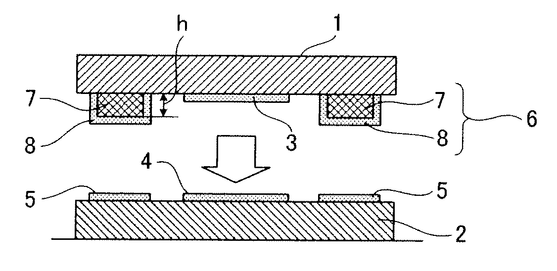
[0044]An electronic part shown in FIG. 1C has a device substrate 1, on which a functional portion is formed, and a bonding substrate 2 bonded together so as to cover each other with a gap d1 therebetween. Furthermore, the functional portion refers to a portion that functions so that the gap d1 changes as a result of applying a force or voltage and the like. More specifically, this electronic part is an electrostatic capacitance detecting type of sensor, and the functional portion is composed such that the central portion of the device substrate 1 is elastically deformed by the action of a force F, and a gap d2 changes between a first detecting electrode 3 provided on the device substrate 1 and a second detecting electrode 4 provided on the bonding substrate 2.

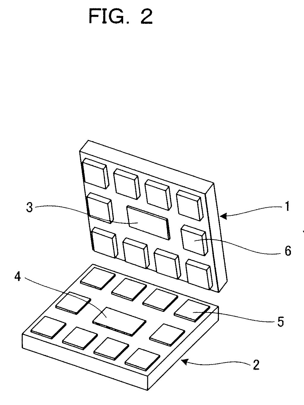
[0045]As shown in FIG. 1A and FIG. 2, a first electrode portion 5 is formed on the bonding substrate 2. A second electrode portion 6 is formed on ...

second embodiment

[0053]FIGS. 3A, 3B and 3C show a second embodiment of the present invention.

[0054]Although Au was used for both the first electrode portion 5 and the bump pattern 8 and both were subjected to direct bonding in the first embodiment, this second embodiment differs from the first embodiment only in that a molten metal 11 such as solder is formed as a bump pattern 8 on the Ni of a core pattern 7 as shown in FIG. 3A.

[0055]When a device substrate 1 and a bonding substrate 2 formed in this manner are clamped between clamping jigs 12a and 12b provided with a heating apparatus as shown in FIG. 3B, and then heated to a temperature equal to or higher than the melting point of the molten metal 11 together with clamping with a load FF, together with the Au of a first electrode portion 5 undergoing plastic deformation, the molten metal 11 becomes a liquid, thereby making it possible to absorb variations in pattern height during bonding and realize stable, high-quality bonding. When cooled while i...

third embodiment

[0057]FIGS. 4A, 4B and 4C show a third embodiment of the present invention.

[0058]Although Au was used for both the first electrode portion 5 and the bump pattern 8 and both were bonded by direct bonding in the first embodiment, this third embodiment differs only in that an electrically conductive adhesive 13, such as a paste in which a fine metal powder such as Ag, Cu or Au is dispersed in an adhesive, is formed as a bump pattern 8 on the Ni of a core pattern 7 as shown in FIG. 4A.

[0059]When a device substrate 1 and a bonding substrate 2 formed in this manner are clamped between clamping jigs 12a and 12b provided with a heating apparatus as shown in FIG. 4B, and then heated to a temperature equal to or higher than the curing temperature of the electrically conductive adhesive 13 together with clamping with load FF, together with the Au of a first electrode portion 5 undergoing plastic deformation, the electrically conductive adhesive 13 is heat-cured, the device substrate 1 and bond...


PUM


Abstract

It is an object of the invention to provide an electronic part capable of forming an accurate gap between opposing substrates while also capable of decreasing the area of the electronic part, and a method of producing the same. A second electrode portion (6), having a core pattern (7) and a bump pattern (8) covering the surface thereof, is provided on a device substrate (1), the core pattern (7) is made of a material having hardness greater than that of the bump pattern (8), a first electrode portion (5) of the same material as the bump pattern (8) is provided on a bonding substrate (2), and a functional portion of the device substrate (1) and the first electrode portion (5) are electrically connected by direct bonding of the first electrode portion (5) and the bump pattern (8).

Description

BACKGROUND OF THE INVENTION[0001]1. Field of the Invention[0002]The present invention relates to an electronic part such as various types of sensors requiring an electrical connection between both opposing substrates and accurate gaps therebetween.[0003]2. Description of the Related Art[0004]In Japanese Patent Application Laid-open No. H3-239940, in the case of mounting a glass substrate 22 on a silicon substrate 21 at a predetermined gap d as shown in FIG. 10, a gap-setting member 24 having a thickness equal to the target gap d is provided bonded separately from a bonding layer 23 that bonds the silicon substrate 21 and the glass substrate 22.[0005]However, in the case of employing the configuration of FIG. 10 for an electronic part, the bonding layer 23 is a low melting point glass-based or chemical-based adhesive, and since an electrical connection cannot be made in the portion of bonding layer 23, it is necessary to form a terminal for making an electrical connection at a differ...

Claims


Application Information

Patent Timeline
IPC IPC(8): H01L23/52H01L21/44
CPCG01D5/2417H01G5/16G01L1/142H01L24/81
Inventor HIGASHI, KAZUSHI
Owner PANASONIC CORP
Why Eureka
Try Eureka