
Photodiodes, image sensing devices and image sensors

Active Publication Date: 2009-06-11
SAMSUNG ELECTRONICS CO LTD
View PDF5 Cites 87 Cited by
  • Summary
  • Abstract
  • Description
  • Claims
  • Application Information

AI Technical Summary

Benefits of technology

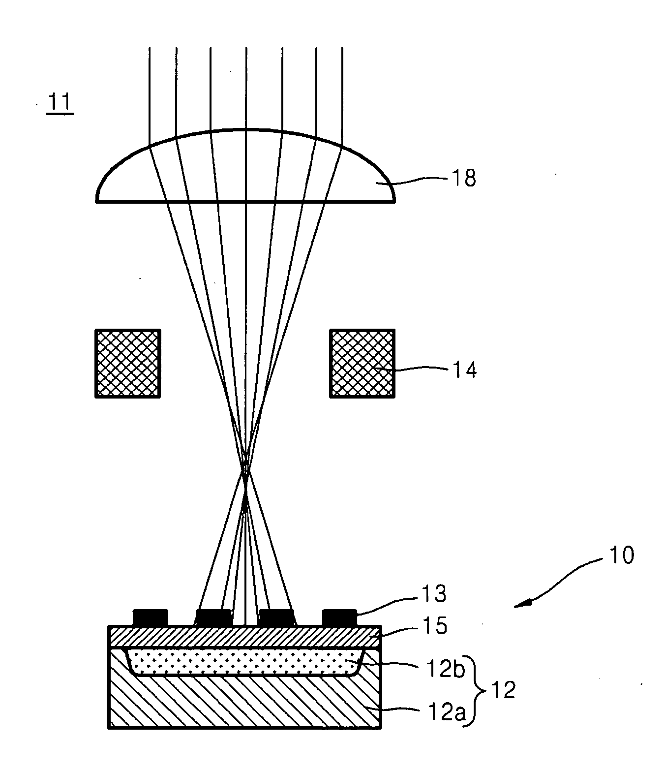
[0012]Example embodiments also may provide a CMOS image sensor having a photodiode. The photodiode may have a metal pattern formed on its surface. The metal pattern may filter light having a particular or given wavelength without an additional color filter. This may increase the amount of light sensed by the image sensor.

Problems solved by technology

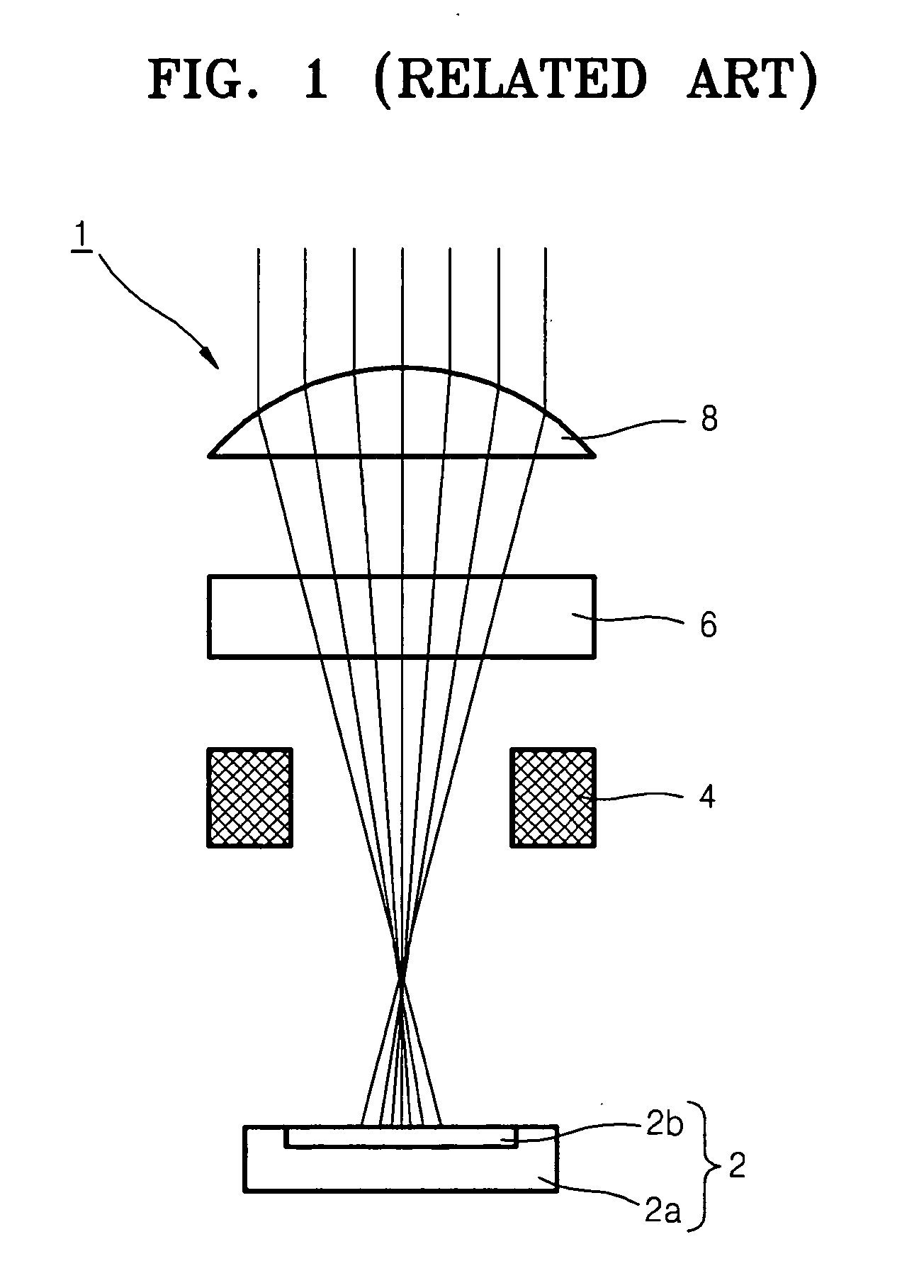
Additionally, because a relatively large amount of light is absorbed while passing through the color filter 6 and the insulating layers, a relatively small amount of light actually reaches the photodiode 2, which may further reduce the sensitivity of the CMOS image sensor.
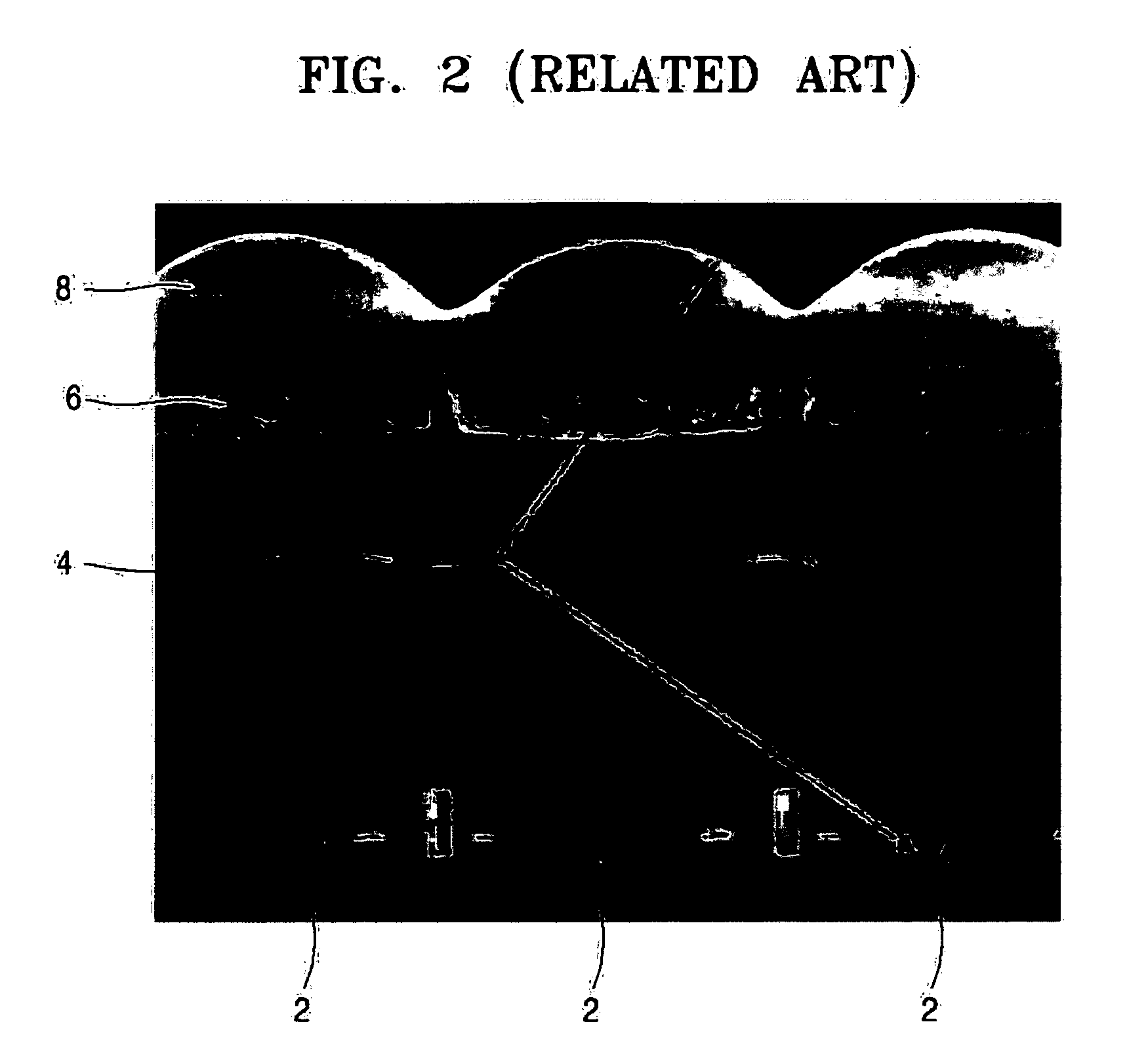
The light entering the adjacent pixel may result in optical cross-talk, which causes signal distortion.
This may increase the amount of light sensed by the image sensor.

Method used


Image

  • Photodiodes, image sensing devices and image sensors
  • Photodiodes, image sensing devices and image sensors
  • Photodiodes, image sensing devices and image sensors

Examples


Embodiment Construction

[0026]Various example embodiments will now be described more fully with reference to the accompanying drawings. However, specific structural and functional details disclosed herein are merely representative for purposes of describing example embodiments, and one skilled in the art will appreciate that example embodiments may be embodied in many alternate forms and should not be construed as limited to only the example embodiments set forth herein.

[0027]It should be understood that, although the terms first, second, etc. may be used herein to describe various elements, these elements should not be limited by these terms. These terms are only used to distinguish one element from another. For example, a first element could be termed a second element, and similarly, a second element could be termed a first element, without departing from the scope of example embodiments. As used herein, the term “and / or” includes any and all combinations of one or more of the associated listed items.

[00...


PUM


Abstract

Provided are photodiodes, image sensing devices and image sensors. An image sensing device includes a p-n junction photodiode having a metal pattern layer on an upper surface thereof. An image sensor includes the image sensing device and a micro-lens formed above the metal pattern layer. The metal pattern layer filters light having a first wavelength.

Description

PRIORITY STATEMENT[0001]This application claims priority under 35 U.S.C. §119 to Korean Patent Application No. 10-2007-0128272, filed on Dec. 11, 2007, in the Korean Intellectual Property Office, the entire contents of which are incorporated herein by reference.BACKGROUNDDescription of the Related Art[0002]A conventional or related art image sensor is a photoelectric conversion device that converts an optical image into an electrical signal by detecting light. Conventional image sensors may be used for storing and transmitting an optical image, and for reproducing the optical image in a display apparatus.[0003]Conventional silicon semiconductor image sensors may be classified as charge coupled device (CCD) image sensors or complementary metal oxide semiconductor (CMOS) image sensors. Conventional CMOS image sensors may have lower production costs using conventional semiconductor manufacturing processes. These manufacturing processes may be simpler, consume less power, and / or periphe...

Claims


Application Information

Patent Timeline
IPC IPC(8): H01L31/113
CPCH01L27/14621H01L31/02165H01L27/14627H01L27/146H01L31/10
Inventor JOE, IN-SUNGPARK, YOON-DONGJIN, YOUNG-GUCHANG, SEUNG-HYUK
Owner SAMSUNG ELECTRONICS CO LTD
Learn More