Method of attenuating an optical signal

Inactive Publication Date: 2005-01-18
SUMITOMO ELECTRIC DEVICE INNOVATIONS U S A
View PDF5 Cites 0 Cited by
  • Summary
  • Abstract
  • Description
  • Claims
  • Application Information

AI Technical Summary

Benefits of technology

When moving a waveguide or optical fiber closer to an optical port of a VCSEL, a more uniform LASER beam profile can be coupled, and the total amount of light gathered will increase. As it is desirable to couple a uniform optical profile, it is not necessarily advantageous to gather as much light as possible. Capturing too much light through an optical fiber or waveguide could cause a few problems, one of whic

Problems solved by technology

As it is desirable to couple a uniform optical profile, it is not necessarily advantageous to gather as much light as possible.
Capturing too much light through an optical fiber or waveguide could cause a few problems, one of which is eye safety.
Another possible consequence in gathering too much light involves the inability of a receiving optical device to process the light energy.
If the in

Method used


Image

  • Method of attenuating an optical signal
  • Method of attenuating an optical signal
  • Method of attenuating an optical signal

Examples


Example

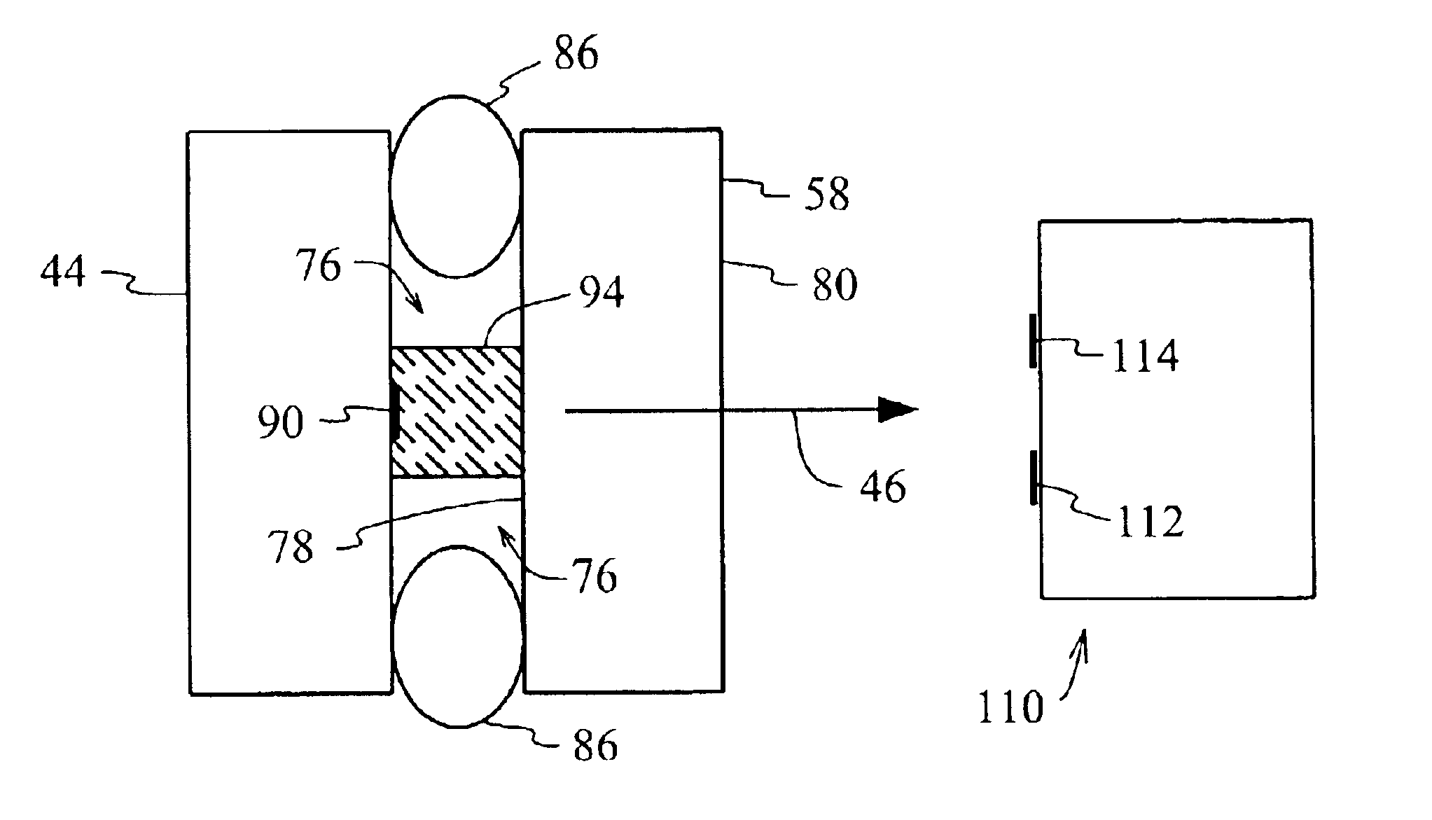
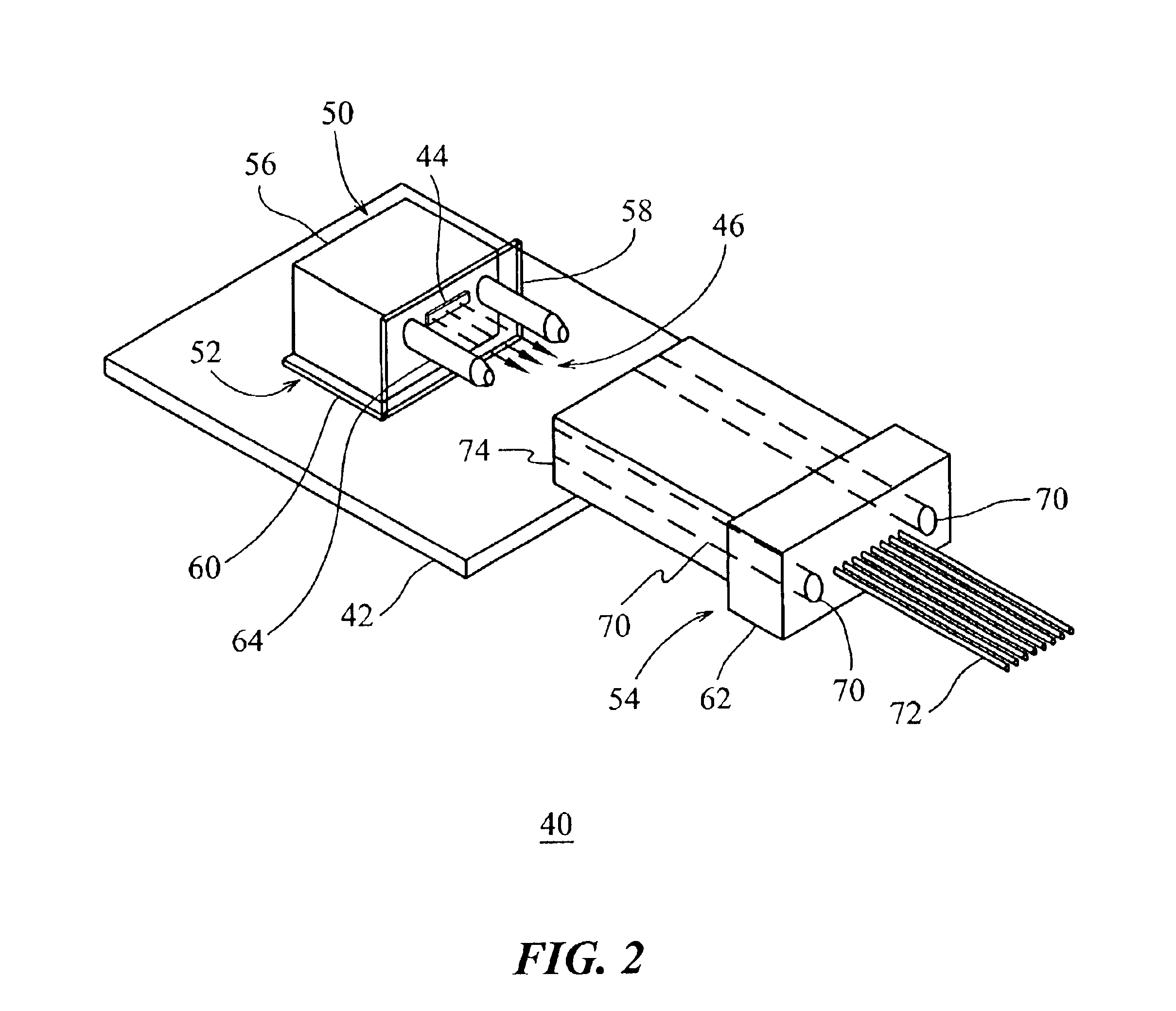
FIG. 2 shows an electro-optic communications assembly 40 in accordance with the invention and in a context of use. The assembly 40 may include a common substrate 42, or printed circuit board (PCB), an optically transparent substrate assembly 52 attached to the PCB 42, and an optical connector assembly 54 generally holding a plurality of optical fibers 72.

The PCB 42, may be any suitable material such as FR4, ceramic interconnect, or the like. The PCB 42 may have a plurality of electrical and optical devices for signal processing, as well as electrical traces and electrical pads (not shown in the figure).

The optically transparent substrate assembly 52 may comprise a glass or a glass-like structure having desirable optical and structural properties, and could be about 110 microns in thickness. The substrate assembly 52 generally includes first and second optically transparent substrates 58, 60 joined along a common edge and an optical array 44. The optical array 44 may be mechanically ...


PUM


Abstract

A method and apparatus are provided for transmitting an optical communications signal. The method includes the steps of securing an optical device onto an optically transparent substrate with an optically transparent adhesive such that an axis of transmission of the optical device passes directly through the optically transparent adhesive and a portion of the body of the optically transparent substrate, darkening a portion of the optically transparent adhesive with a laser; and transmitting light from the optical device through the darkened portion of the optically transparent adhesive such that at least some of the light from the optical device is absorbed by the darkened portion.

Description

FIELD OF THE INVENTIONThe present invention relates to optical communication devices, and more specifically to the structure of opto-electronic couplers.BACKGROUND OF THE INVENTIONThis application claims the benefit of U.S. Provisional Patent Application No. 60 / 317,138, filed on Sep. 6, 2001.Traditionally, VCSEL dies are vertically mounted to a printed circuit board, or PCB, with light emitting from the same surface as the electrical contacts. The PCB is usually made of FR4 or ceramic. As shown in the prior art of FIG. 1, a TO can 12 has wire bonds 16 used in electrically connecting the VCSEL die 14. Wire bonds 16 are more susceptible to damage than solder bumps, and are generally avoided if possible. In addition, wire bonding is inconsistent in terms of variance in electrical properties. As the wire lengths vary, the resistance, inductance and capacitance also varies.As shown in FIG. 1, the TO can's base comprises a header 20 and a conductive spacer 18. A metallic structure 22, ref...

Claims


Application Information

Patent Timeline
IPC IPC(8): G02B6/42
CPCG02B6/4206G02B6/4249G02B6/4292H01L2224/48091H01L2924/30107H01L2924/12041H01L2924/00014H01L2924/00
Inventor WICKMAN, RANDY W.BROCKMAN, THOMASNELSON, STEVEN C.
Owner SUMITOMO ELECTRIC DEVICE INNOVATIONS U S A
Why Eureka
Try Eureka