

Radiation-Emitting Semiconductor Chip
- Summary
- Abstract
- Description
- Claims
- Application Information
AI Technical Summary
Benefits of technology
Problems solved by technology
Method used
Image

Examples
Embodiment Construction
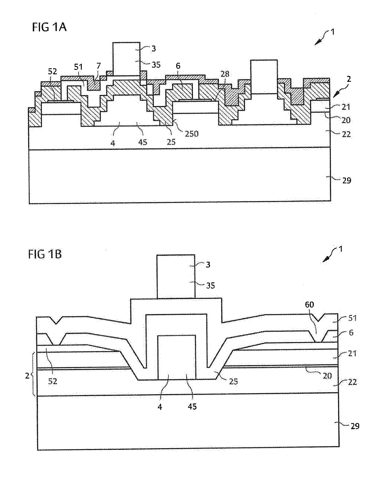
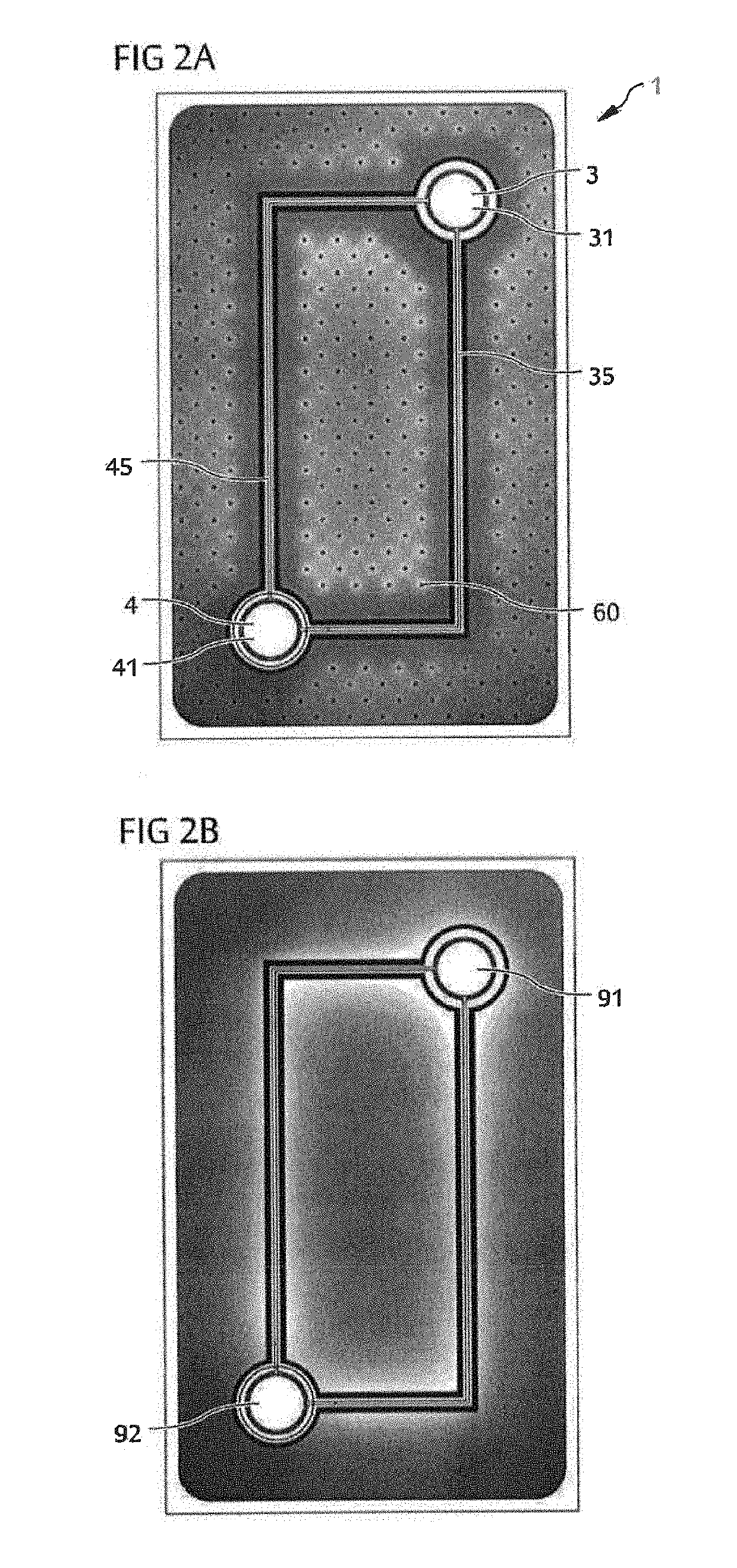
[0067]FIG. 1A shows a first exemplary embodiment of a radiation-emitting semiconductor chip 1, wherein FIG. 1B shows a section of said semiconductor chip in a sectional view. In plan view, the radiation-emitting semiconductor chip can be formed, for example, as shown in FIG. 2A.
[0068]The radiation-emitting semiconductor chip 1 has a semiconductor body 2 with a semiconductor layer sequence. The semiconductor body 2 comprises in particular an active region 20 intended for generating radiation, which is arranged between a first semiconductor layer 21 of a first conductivity type (for example, p-conducting) and a second semiconductor layer 22 of a second conductivity type different from the first conductivity type (for example, n-conducting). The semiconductor body 2, in particular the active region 20, is preferably based on a III-V compound semiconductor material, in particular on a nitride compound semiconductor material.
[0069]“Based on nitride compound semiconductor material” in the...
PUM
 Abstract
Description
Claims
Application Information