Unlock instant, AI-driven research and patent intelligence for your innovation.

NAND flash memory and memory system

a technology of flash memory and memory system, applied in the field of nand flash memory and a memory system, can solve the problems of data being erroneously read, increasing the probability of erroneous writing, and more likely to occur erroneous writing

Inactive Publication Date: 2009-06-11
KK TOSHIBA
View PDF6 Cites 22 Cited by
  • Summary
  • Abstract
  • Description
  • Claims
  • Application Information

AI Technical Summary

Problems solved by technology

Thus the data is erroneously read and problems occur when the data is held.
Even if the threshold voltage can be set at a higher threshold distribution to write data, the probability of erroneous writing may increase.
Although binary or four-valued data is not disadvantageous, octal or hexadecimal data is more likely to cause some problems when the data is held.
The same problem may occur between the drain-side selection transistor SGD and the memory cell M31.
Consequently, erroneous writing is more likely to occur.

Method used


Image

  • NAND flash memory and memory system
  • NAND flash memory and memory system
  • NAND flash memory and memory system

Examples


first embodiment

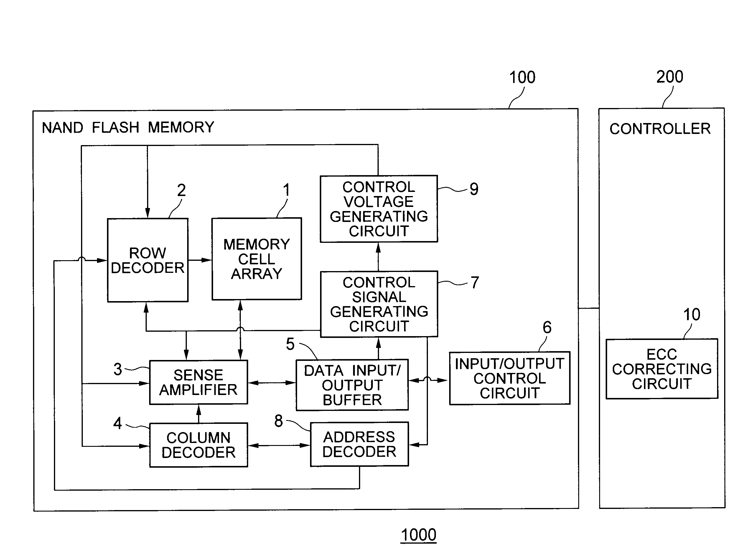
[0041]FIG. 1 is a block diagram showing the main configuration of a memory system 1000 according to a first embodiment which is an aspect of the present invention. FIG. 2 illustrates the configuration of a memory cell array 1 shown in FIG. 1. FIG. 3 is a circuit diagram showing the main configuration of a block of the memory cell array 1 shown in FIG. 2.

[0042]As shown in FIG. 1, the memory system 1000 includes a NAND flash memory 100 and a controller 200.

[0043]The NAND flash memory 100 includes the memory cell array 1, a row decoder 2, a sense amplifier 3, a column decoder 4, a data input / output buffer 5, an input / output control circuit 6, a control signal generating circuit 7, an address decoder 8, and a control voltage generating circuit 9.

[0044]The controller 200 includes an ECC correcting circuit 10.

[0045]As shown in FIG. 2, the memory cell array 1 is made up of a plurality of blocks 11 which are units of writing / deletion of data.

[0046]For example, the block 11 includes, as show...


PUM


Abstract

A NAND flash memory comprising blocks which are units of writing and deletion of data, the block comprising: memory cells from which data corresponding to values of held threshold voltages can be read by applying a reading voltage to control gates of the memory cells; source-side selection gate transistors connected between a common source line and the memory cells; drain-side selection gate transistors connected between a bit line and the memory cells; and monitor cells which are configured as the memory cells and have a threshold voltage set according to monitor data, and from which data corresponding to values of held threshold voltages can be read by applying a decision voltage to control gates of the monitor cells.

Description

CROSS-REFERENCE TO RELATED APPLICATION[0001]This application is based upon and claims the benefit of priority from the prior Japanese Patent Application No. 2007-315549, filed on Dec. 6, 2007, the entire contents of which are incorporated herein by reference.BACKGROUND OF THE INVENTION[0002]1. Field of the Invention[0003]The present invention relates to a NAND flash memory and a memory system.[0004]2. Background Art[0005]In a nonvolatile memory cell of a NAND flash memory and so on, electrons are trapped in an oxide film by applying a high electric field. Thus the threshold voltage of the memory cell is changed and data is written according to the threshold voltage, and then the data is read using a difference in the threshold voltage.[0006]When the electrons are permanently trapped in the oxide film, the data is held without any problems. However, the electrons trapped in the oxide film are drawn to a stable neutral threshold voltage with the passage of time.[0007]The drawing of el...

Claims


Application Information

Patent Timeline
Patent Type & Authority Applications(United States)
IPC IPC(8): G11C16/06G11C8/00G11C7/00
CPCG11C8/08G11C8/12G11C29/00G11C16/3418G11C16/3431G11C11/5621G11C16/02G11C16/30G11C16/08G11C16/34
Inventor ISOBE, KATSUAKI
Owner KK TOSHIBA