
Sense amplifier and driving method thereof, and semiconductor memory device having the sense amplifier

a technology of sense amplifier and driving method, which is applied in the direction of information storage, static storage, digital storage, etc., can solve the problems of data error in the output deterioration of the operational characteristics of the sense amplifier, etc., and achieve the effect of increasing the layout of the semiconductor memory device and improving driving capability

Inactive Publication Date: 2009-06-11
SK HYNIX INC
View PDF4 Cites 21 Cited by
  • Summary
  • Abstract
  • Description
  • Claims
  • Application Information

AI Technical Summary

Benefits of technology

[0024]According to the present invention, the sense amplifier can sense data without being influenced by the offset characteristic by performing the negative pull down drive and the overdrive.
[0025]Further, the semiconductor memory device according to the present invention can compensate driving capability by causing the negative drive voltage generating unit to supply driving voltage to the sense amplifier independently during an active operation and sharing voltage having the same voltage level with the back bias voltage generating unit (which provides back bias to the cell array) in the refresh mode where driving voltage is largely consumed due to successive active operations.
[0026]Additionally, the semiconductor memory device according to the present invention improves driving capability without increasing the layout of the semiconductor memory device by compensating driving capability by sharing the voltage between a back bias voltage generating unit and a negative voltage generating unit.

Problems solved by technology

However, the semiconductor memory device described above causes the margin of the operation voltage for the threshold voltage to be reduced if the operation voltage is lowered, thereby deteriorating the operational characteristics of the sense amplifier.
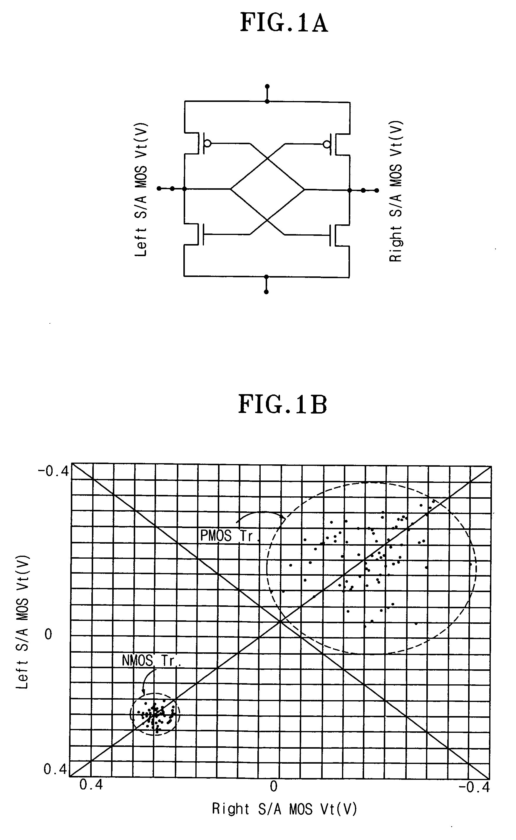
However, a problem occurs which causes a data error in the output of the sense amplifier due to the great influence of the offset characteristic of the PMOS transistor.

Method used


Image

  • Sense amplifier and driving method thereof, and semiconductor memory device having the sense amplifier
  • Sense amplifier and driving method thereof, and semiconductor memory device having the sense amplifier
  • Sense amplifier and driving method thereof, and semiconductor memory device having the sense amplifier

Examples


Embodiment Construction

[0034]Hereinafter, preferred embodiments of the present invention will be described in detail with reference to the accompanying drawings.

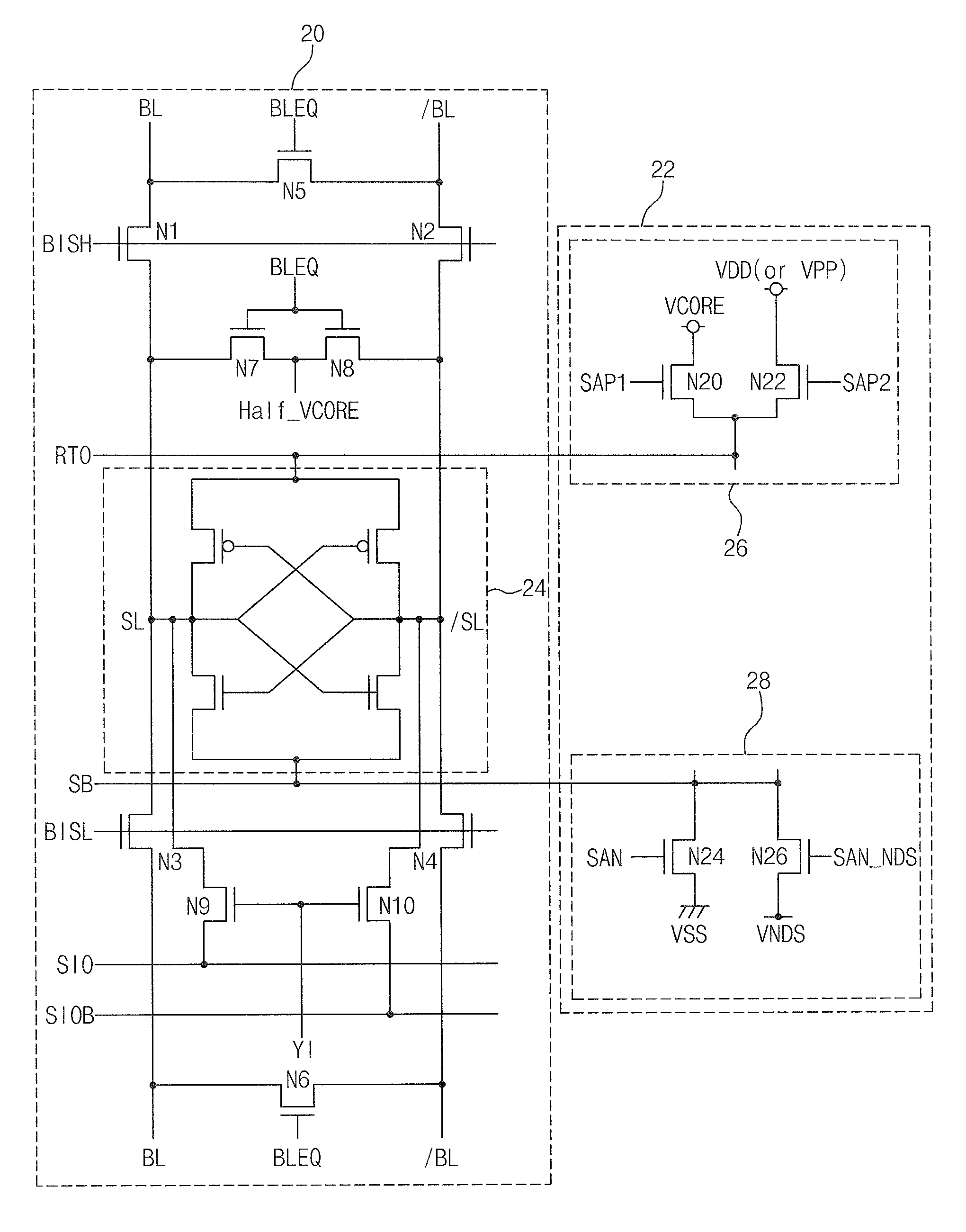
[0035]FIG. 3 is a diagram showing a cell array 10 and a sensing related block. The present invention exemplifies a cell array 10 having a folded bit line structure and a latch-type sense amplifier 12.

[0036]The cell array 10 includes DRAM cells each composed of one NMOS transistor T and one capacitor CS that is adjusted by a word line WL. Each cell in the cell array corresponds to one of the word lines WL0, WL1, WL2, WL3, WL4, and WL5. The drain of the NMOS transistor T of a cell is connected to the bit line BL, / BL, and the source is connected to an electrode of the corresponding capacitor CS. The node at the connection between the NMOS transistor T1 and the capacitor CS is defined as a storage node SN and the storage node SN includes the charge written to the cell as data. The node of the capacitor CS opposite the storage node SN functions as a p...


PUM


Abstract

The semiconductor memory device includes a bank having a cell array and a sense amplifier. A back bias voltage generating unit supplies a back bias voltage to the cell array of the bank. A negative drive voltage generating unit generates negative driving voltages including a normal pull-up voltage, an overdrive voltage, a normal pull-down voltage, and a negative voltage and supplies the negative driving voltages to the sense amplifier of the bank. A switching unit opens a connection between the back bias voltage generating unit and the negative drive voltage generating unit when in active mode and shares the back bias voltage between the back bias voltage generating unit and the negative drive voltage generating unit when in a refresh mode, in response to an external command.

Description

CROSS-REFERENCE TO RELATED APPLICATIONS[0001]The present application claims priority to Korean patent application number 10-2007-0125389 filed on Dec. 5, 2006 which is incorporated herein by reference in its entirety.BACKGROUND OF THE INVENTION[0002]The present invention relates generally to a semiconductor memory device, and more particularly to a sense amplifier performing a negative drive, a driving method of the sense amplifier performing a pull-down drive by a negative voltage, and a semiconductor memory device having the sense amplifier.[0003]The data to be stored in a cell array or the data stored in the cell array is carried on a bit line of the semiconductor memory device. The data delivered between the bit line and a data bus is sensed and amplified by a sense amplifier.[0004]The structure of a cross-coupled latch-type sense amplifier is shown in FIG. 1a. FIG. 1B shows the threshold voltage offset characteristic of a NMOS transistor and a PMOS transistor provided in the se...

Claims


Application Information

Patent Timeline
IPC IPC(8): G11C7/08
CPCG11C11/4091G11C7/08G11C7/06G11C5/14
Inventor KANG, HEE BOK
Owner SK HYNIX INC
Learn More