Manufacturing method for a card and card obtained by said method

a manufacturing method and card technology, applied in the field of cards, can solve the problems of internal mechanical stress, delamination, deformation of cards, and inability to make milling steps, and achieve the effect of improving the process of making chip cards

Inactive Publication Date: 2009-06-18
ASSA ABLOY AB
View PDF14 Cites 32 Cited by
  • Summary
  • Abstract
  • Description
  • Claims
  • Application Information

AI Technical Summary

Benefits of technology

[0023]It is an aim of the present invention to improve the proce

Problems solved by technology

Milling steps are however not practical and have many drawbacks.
For example, they induce internal mechanical stress in the laminated layers which may end in defects, delamination, deformation of the card etc.
Technically, the milling is very difficult to carry out in order to avoid misalignment or damaging the contact portion of the antenna for example.
Hence, due to these milling steps, such cards are produced only one by one which is expensive and time consuming.
The insertion of a chip module in a laminated card is a weak point in that the chip module is

Method used


Image

  • Manufacturing method for a card and card obtained by said method
  • Manufacturing method for a card and card obtained by said method
  • Manufacturing method for a card and card obtained by said method

Examples


Embodiment Construction

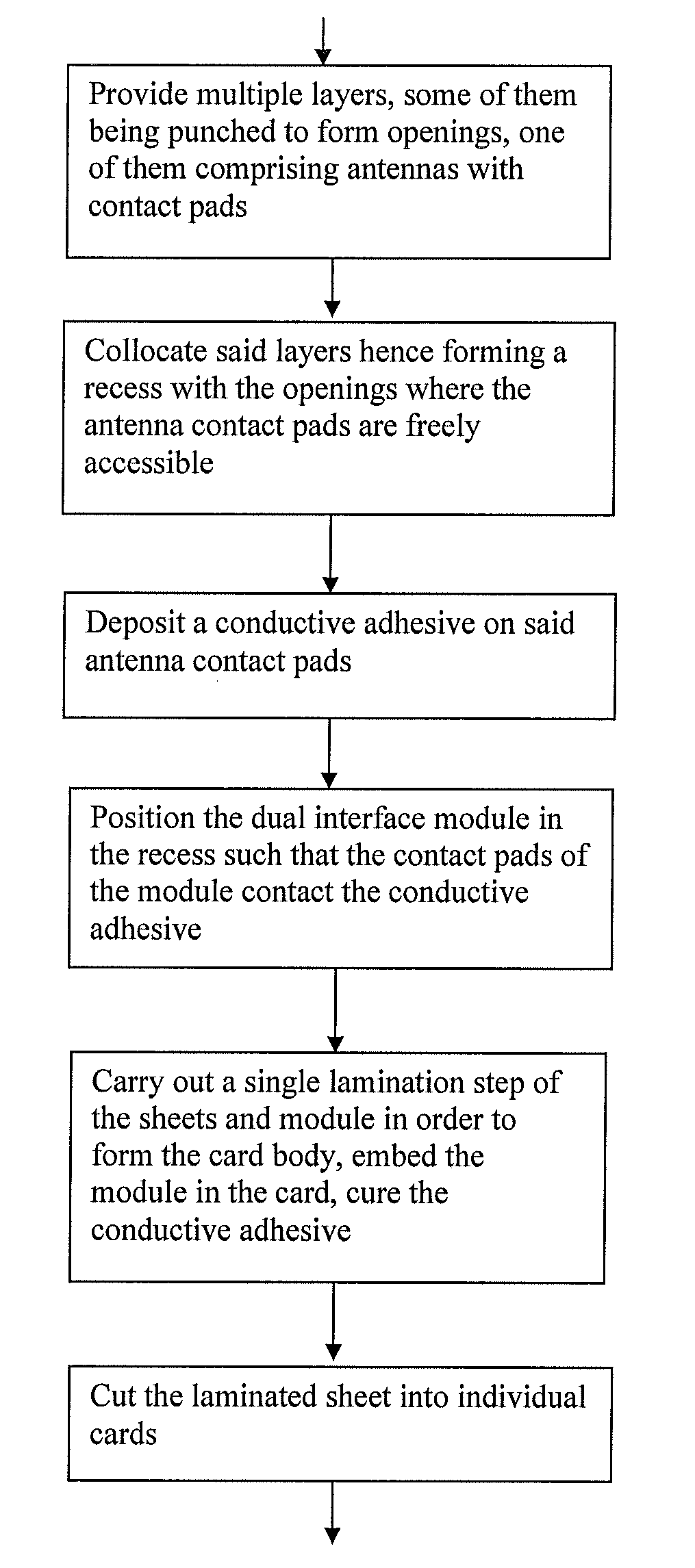
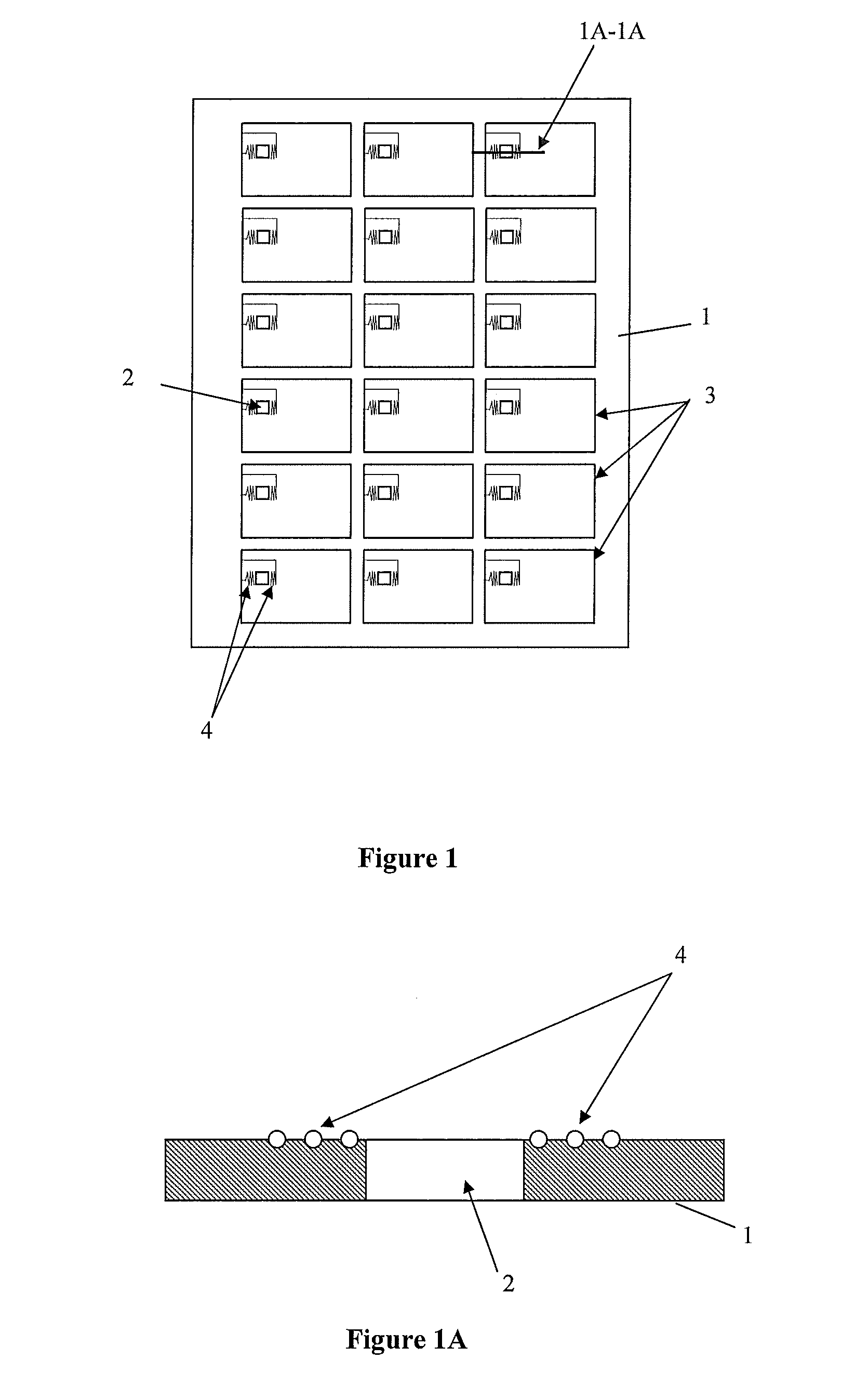
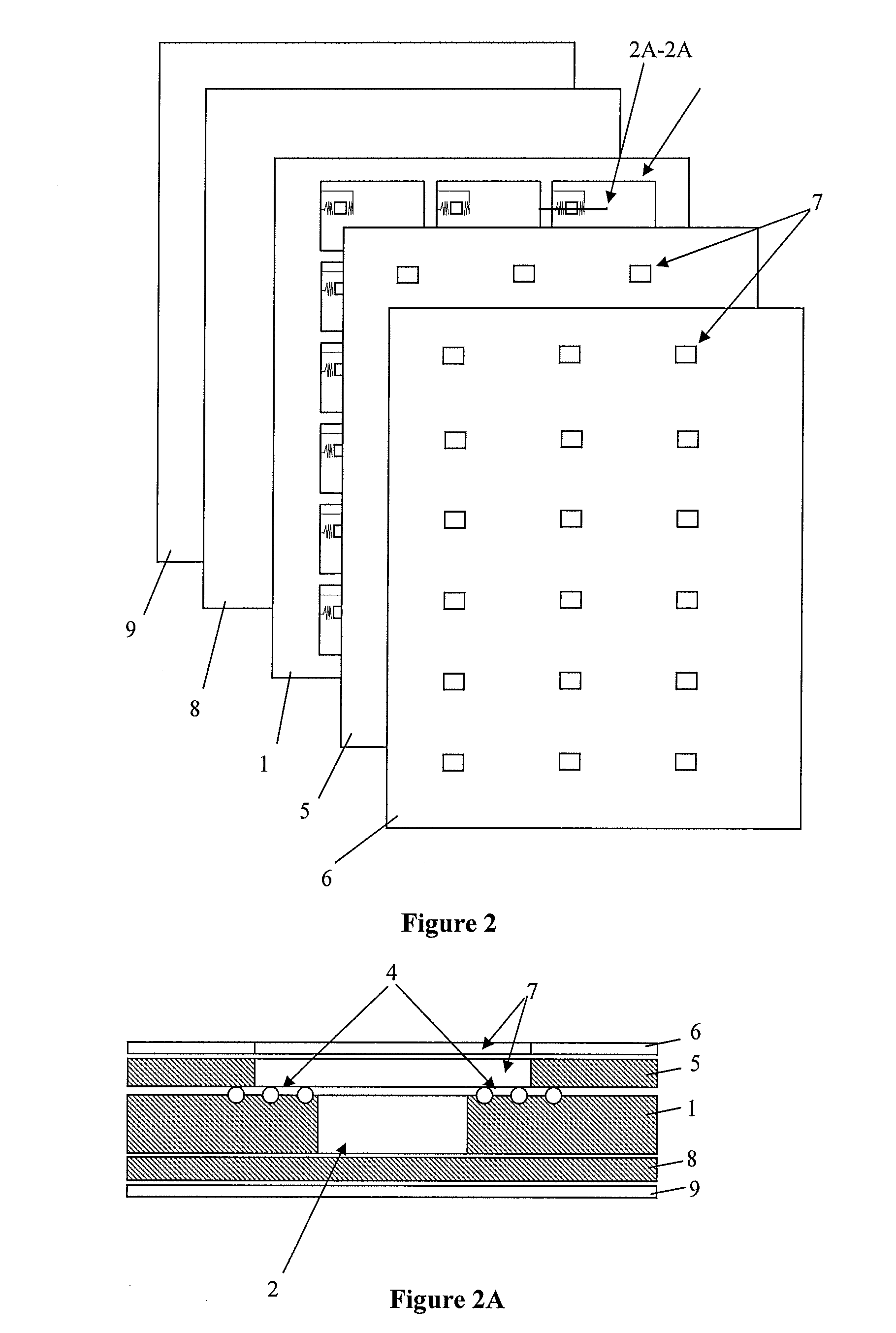
[0048]FIG. 1 shows an initial step of the process. A sheet or layer of material 1 is punched according to the top size of the module (described in more detail further down in the present specification) to form openings 2 in the layer 1. Typically, said sheet 1 comprises several openings 2 punched in a matrix like arrangement of lines and columns in order to be able to fabricate several cards at the same time with the same piece. Once the cards have been built, the sheets will be cut into individual cards.

[0049]The thickness of this sheet 1 will be higher than the thickness of the glob top protection associated with the module.

[0050]This material can be PVC, PC, or any other common plastic used in the smart card industry. As said, this sheet, also called format, will support several dual interface card locations in a matrix-like arrangement.

[0051]FIG. 1A shows a partial cross section of the opening 2. This cross-section corresponds for example to the opening that is placed on the top...


PUM

PropertyMeasurementUnit
Temperatureaaaaaaaaaa
Electrical conductoraaaaaaaaaa
Timeaaaaaaaaaa

Abstract

A method for manufacturing a dual interface card includes at least the following step:
    • collocating multiple card support sheets one onto the other, some of these sheets showing holes, in order to form a recess adapted to receive the dual interface module, one of the sheets supporting the antenna having solid metallic contact pads at least partially freely accessible in the recess
    • depositing a conductive adhesive onto the contact pads
    • positioning the dual interface module in the recess such that the pads of the module are contacting the conductive adhesive
    • executing one single lamination step of the sheets with the module in order to:
      • laminate the multiple layers together in order to form the card body
      • embed the dual interface module in the recess and
      • achieve the curing of the isotropic conductive adhesive and the permanent electrical contact between the antenna and the dual interface module.

Description

TECHNICAL FIELD[0001]The present invention concerns a manufacturing method for cards with a dual interface module showing free contact electrodes at the surface of the card for a contact-type communication, and pads connected to an antenna embedded in the card body for a contactless-type communication. These cards are called dual interface cards.[0002]The present invention also concerns a card obtained by the method steps of the invention.BACKGROUND ART[0003]Such dual interface cards (contact / contactless) are known in the prior art. In the field of fabricating such cards, it has been usual to laminate several layers of material forming a card with an antenna (for example a wire antenna) embedded in the card body for the contactless communication.[0004]Once a card element has been prepared, it is necessary to create a recess in the card element, usually by milling, in order to form the space in which a chip module is to be inserted and to free the contact portions of the antenna whic...

Claims


Application Information

Patent Timeline
IPC IPC(8): H05K3/00H01P11/00
CPCH05K2201/10287Y10T29/49124Y10T29/49002H05K3/321G06K19/07745H05K2201/10727H01L2924/0002H05K3/103Y10T29/49016H05K1/183G06K19/07749H01L2924/00
Inventor AYALA, STEPHANECARRE, LIONELCURTY, JARI-PASCAL
Owner ASSA ABLOY AB
Why Eureka
Try Eureka