

Manufacturing method of thin film transistor and manufacturing method of display device
- Summary
- Abstract
- Description
- Claims
- Application Information
AI Technical Summary
Benefits of technology
Problems solved by technology
Method used
Image

Examples
embodiment mode 1
[0079]In Embodiment Mode 1, an example of a manufacturing method of a thin film transistor and a manufacturing method of a display device in which the thin film transistors are arranged in matrix will be described with reference to FIG. 1A to FIG. 25B-2.
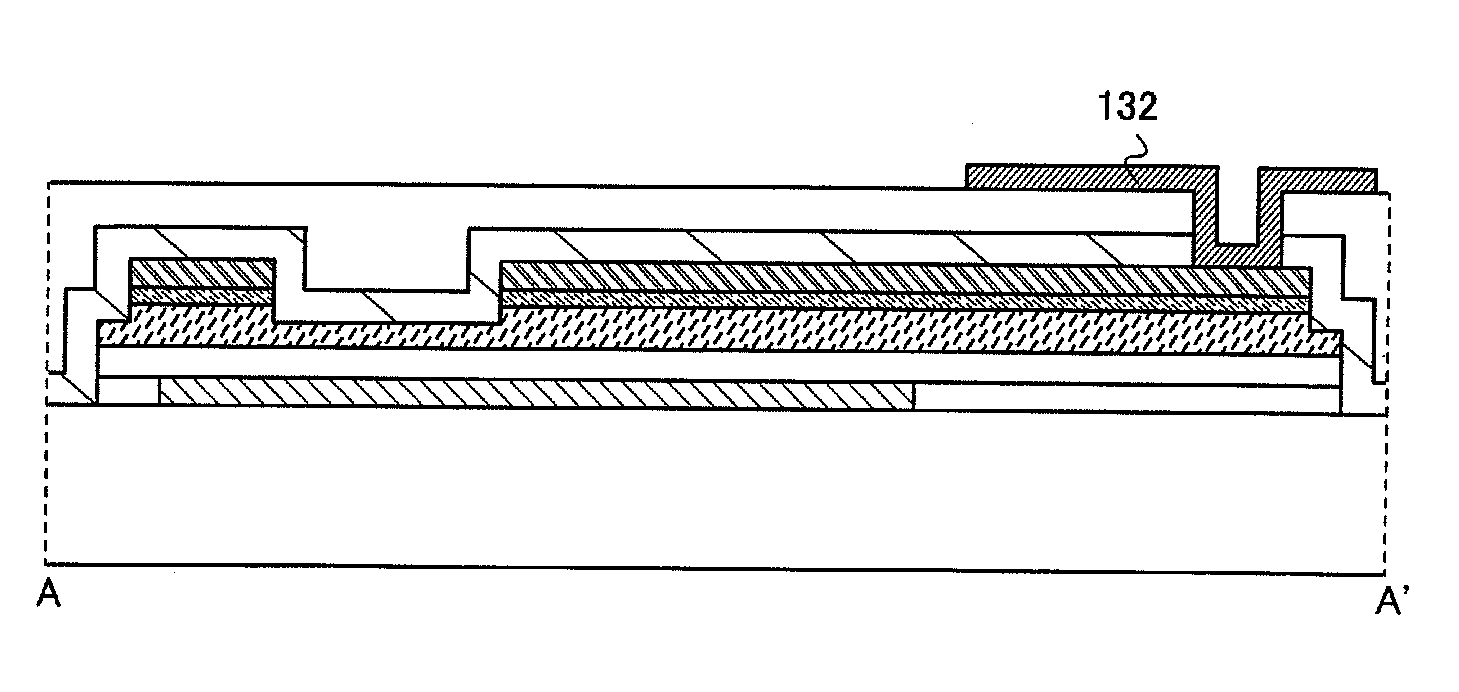
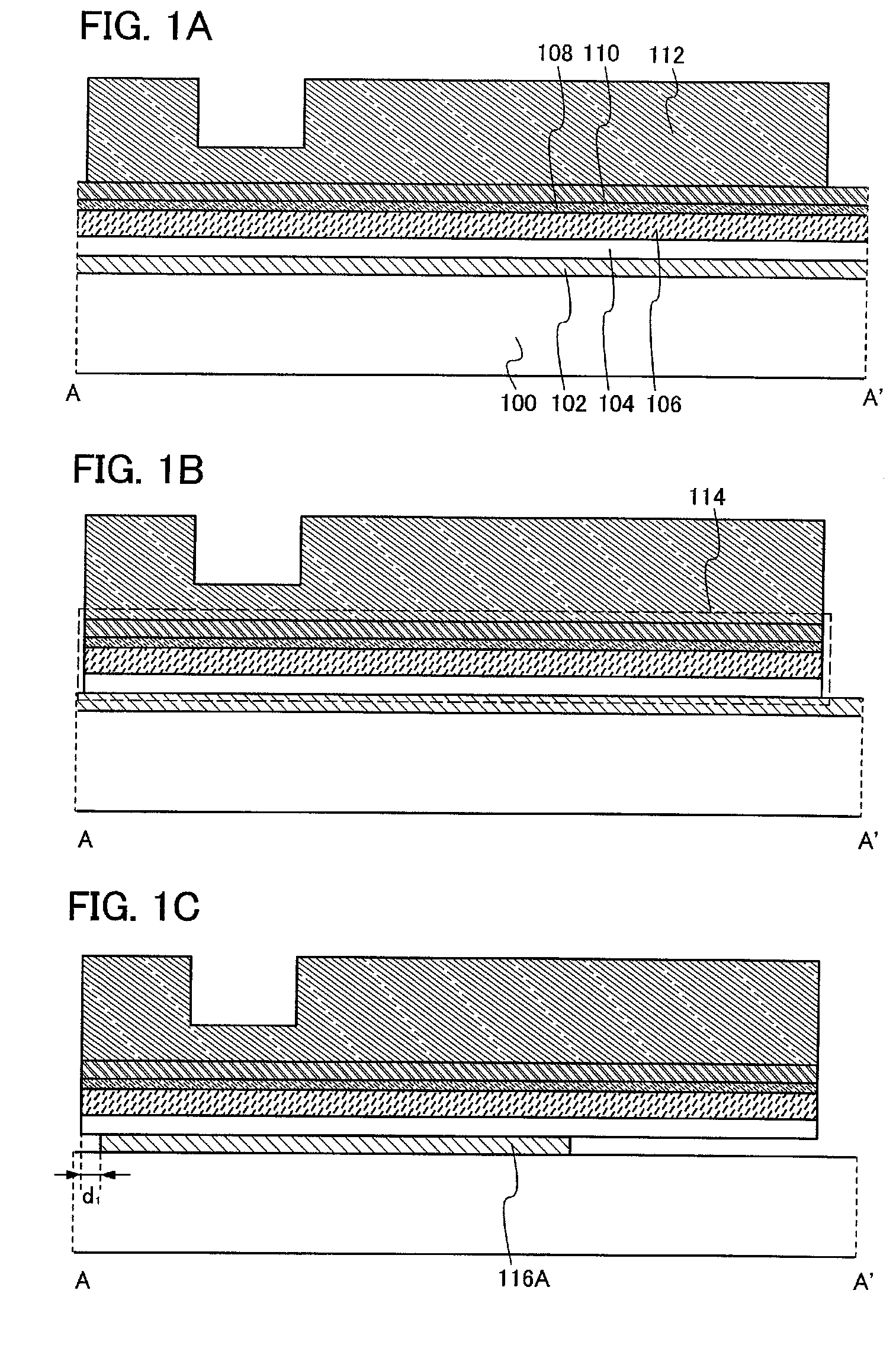
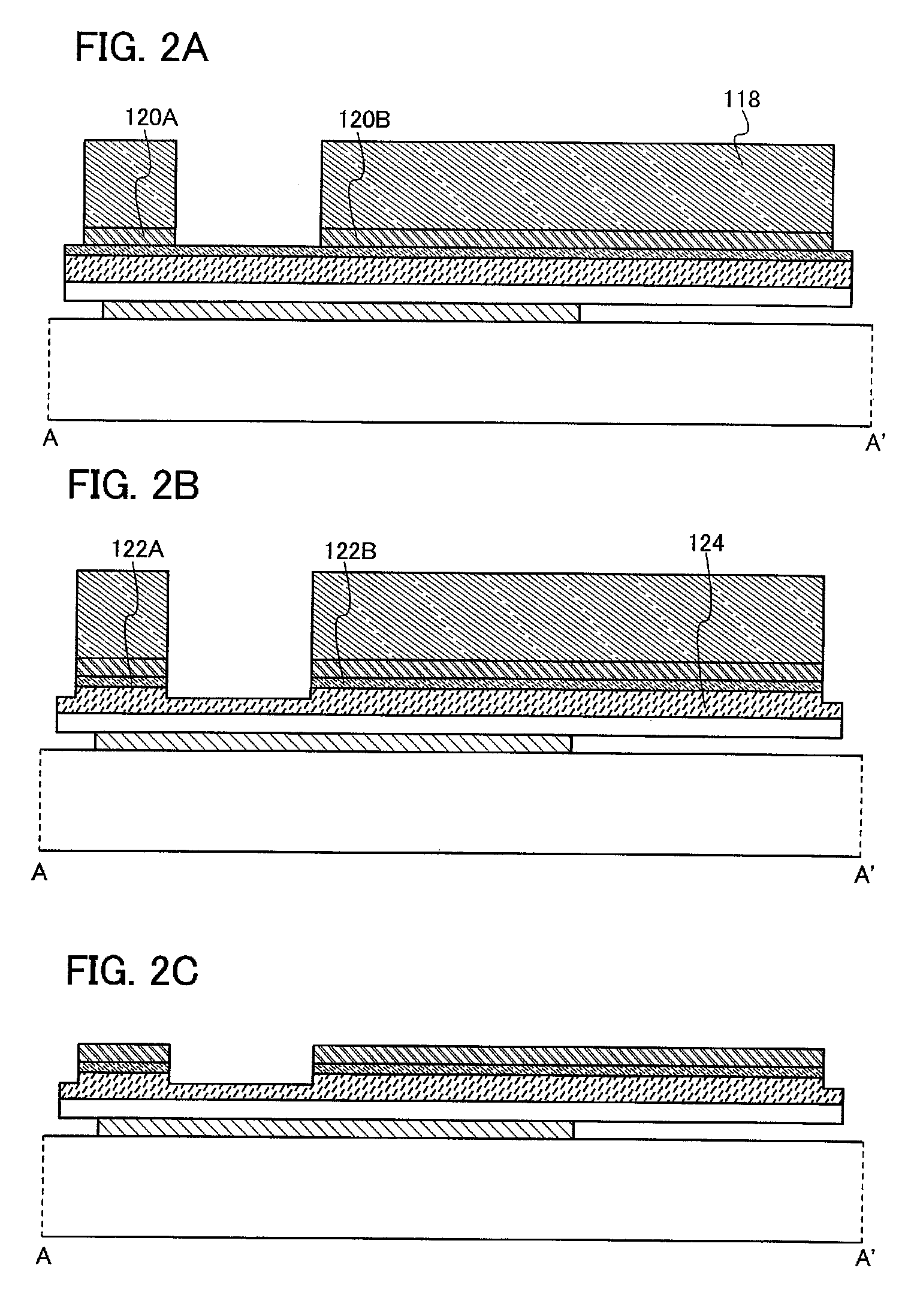
[0080]FIG. 16 to FIG. 20 are top views of thin film transistors according to this embodiment mode. FIG. 20 is a completion drawing in the situation that formation of a pixel electrode is finished. FIG. 1A to FIG. 3C are cross-sectional views taken along the line A-A in FIG. 16 to FIG. 20. FIG. 4A to FIG. 6C are cross-sectional views taken along the line B-B′ in FIG. 16 to FIG. 20. FIG. 7A to 9C are cross-sectional views taken along the line C-C′ in FIG. 16 to FIG. 20. FIG. 10A to FIG. 12C are cross-sectional views taken along the line D-D′ in FIG. 16 to FIG. 20. FIG. 13A to FIG. 15C are cross-sectional views taken along the line E-E′ in FIG. 16 to FIG. 20.
[0081]First, a first conductive film 102, a first insulating film 104, a semico...
embodiment mode 2
[0176]In Embodiment Mode 2, a manufacturing method of a thin film transistor and a manufacturing method of a display device according to the present invention, which are different from those of Embodiment Mode 1, will be described. Specifically, a manufacturing method of a thin film transistor which is similar to that of Embodiment Mode 1, without using a multi-tone mask will be described with reference to FIGS. 26A, 26B, and 26C, FIGS. 27A, 27B, and 27C, FIG. 28, FIG. 29, and FIG. 30.
[0177]FIGS. 26A, 26B, and 26C correspond to FIG. 1A, FIG. 1C, and FIG. 2A of Embodiment Mode 1. FIGS. 27A, 27B, and 27C correspond to FIG. 10A, FIG. 10C, and FIG. 11A of Embodiment Mode 1. FIG. 28, FIG. 29, and FIG. 30 correspond to FIG. 16, FIG. 17, and FIG. 18 of Embodiment Mode 1. The cross-sectional views taken along the line A-A′ illustrated in FIG. 28, FIG. 29, and FIG. 30 correspond to FIGS. 26A, 26B, and 26C, and the cross-sectional views taken along the line D-D′ illustrated in FIG. 28, FIG. 2...
embodiment mode 3
[0187]In Embodiment Mode 3, a manufacturing method of a thin film transistor and a manufacturing method of a display device according to the present invention, which are different from those of Embodiment Modes 1 and 2, will be described. Specifically, a mode in which a first conductive film 102 is etched by the first etching which is described in Embodiment Modes 1 and 2 will be described with reference to FIGS. 31A to 31C, FIGS. 32A to 32C, FIGS. 33A to 33C, FIGS. 34A to 34C, FIGS. 35A to 35C, and FIG. 36.
[0188]FIGS. 31A to 31C correspond to FIGS. 1A to 1C of Embodiment Mode 1. FIGS. 32A to 32C correspond to FIGS. 4A to 4C of Embodiment Mode 1. FIGS. 33A to 33C correspond to FIGS. 7A to 7C of Embodiment Mode 1. FIGS. 34A to 34C correspond to FIGS. 10A to 10C of Embodiment Mode 1. FIGS. 35A to 35C correspond to FIGS. 13A to 13C of Embodiment Mode 1. FIG. 36 corresponds to FIG. 16 of Embodiment Mode 1.
[0189]First, similar to Embodiment Mode 1, a first conductive film 102, a first in...
PUM
 Abstract
Description
Claims
Application Information