Semiconductor integrated circuits including grating coupler for optical communication and methods of forming the same

Inactive Publication Date: 2009-06-18
ELECTRONICS & TELECOMM RES INST
View PDF15 Cites 23 Cited by
  • Summary
  • Abstract
  • Description
  • Claims
  • Application Information

AI Technical Summary

Benefits of technology

[0042]According to the present invention, at least one reflector is formed below a grating through an ion implantation process. Accordingly, a portion of an optical signal that is transmitted below an optical waveguide is reflected toward the optical wave guide by the reflector. Accordingly, an optic

Problems solved by technology

However, communication speed between semiconductor integrated circuits or semiconductor integrated circuits and other electronic medium reaches the limitations due to high electrical resistan

Method used


Image

  • Semiconductor integrated circuits including grating coupler for optical communication and methods of forming the same
  • Semiconductor integrated circuits including grating coupler for optical communication and methods of forming the same
  • Semiconductor integrated circuits including grating coupler for optical communication and methods of forming the same

Examples


first embodiment

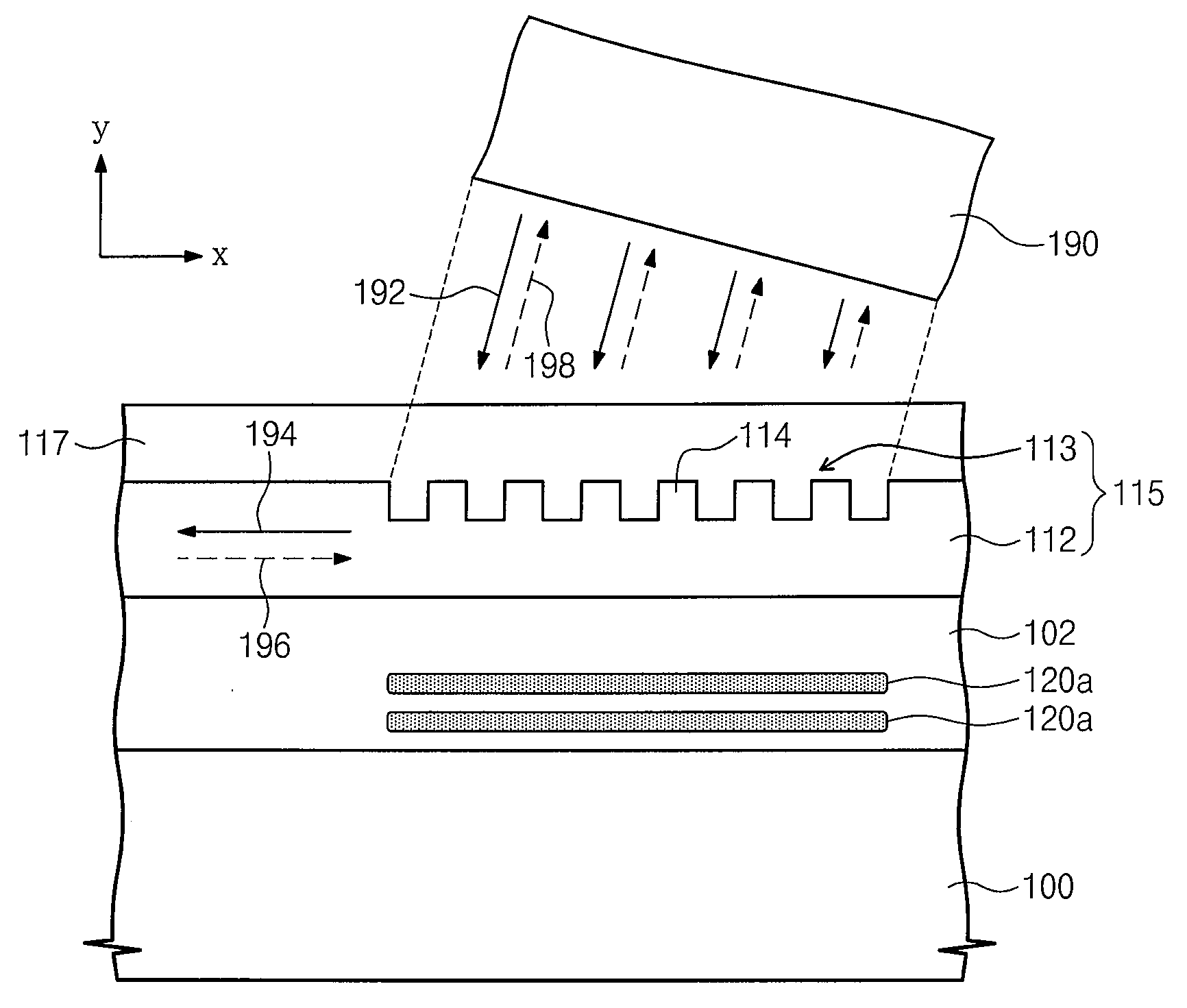
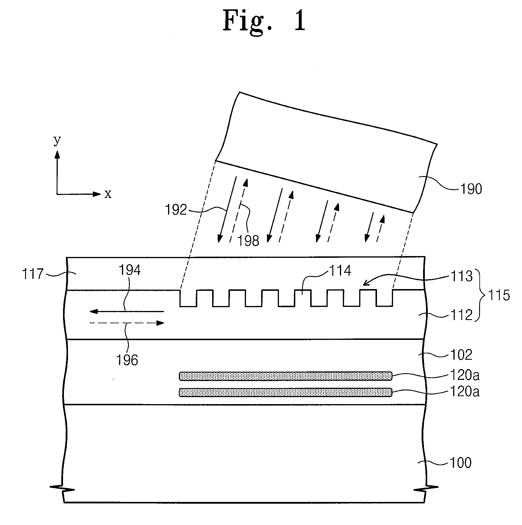
[0066]FIG. 1 is a sectional view of a semiconductor integrated circuit including a grating coupler according to one embodiment of the present invention.

[0067]Referring to FIG. 1, a cladding layer 102 is disposed on a semiconductor substrate 100. A grating coupler 115 is disposed on the cladding layer 102. The grating coupler 115 includes an optical waveguide 112 on the cladding layer 102 and a grating 113 on the optical waveguide 112. The optical waveguide 112 extends along one direction parallel to the top surface of the semiconductor substrate 100. The one direction corresponds to an x-axis direction of FIG. 1. A y-axis direction of FIG. 1 corresponds to a direction vertical to the top surface of the semiconductor substrate 100. The grating 113 includes a plurality of protrusions 114 spaced apart from each other in the one direction. The grating 113 is formed by the spaced protrusions 114. Both sidewalls of the protrusions 114 may be vertical to the top surface of the semiconducto...

second embodiment

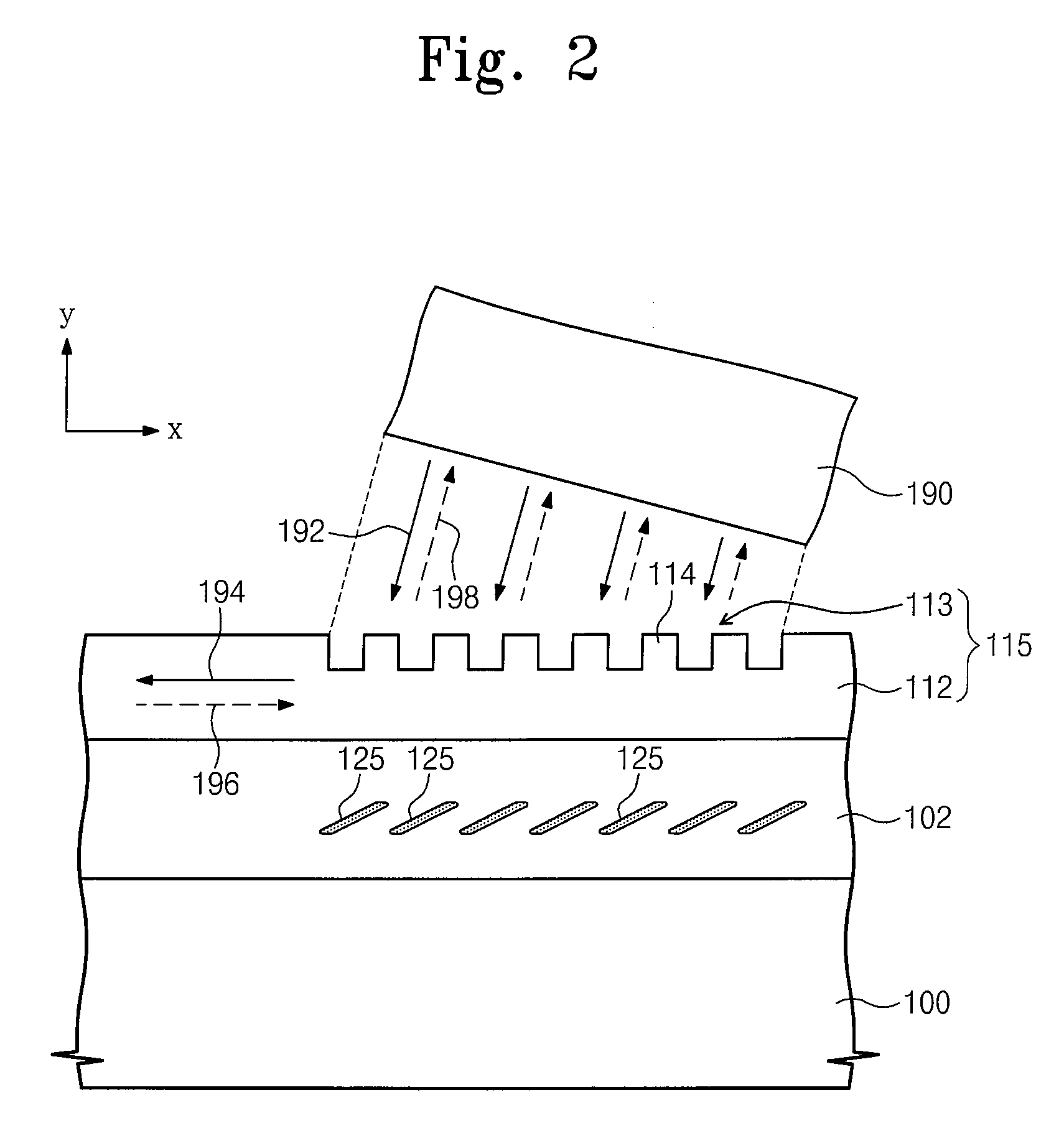
[0120]A semiconductor integrated circuit according to the second embodiment of the present invention includes a reflector in a semiconductor substrate. Like reference numerals refer to like elements throughout.

[0121]FIG. 9 is a sectional view of a semiconductor integrated circuit including a grating coupler according to another embodiment of the present invention.

[0122]Referring to FIG. 9, a cladding layer 102 is disposed on a semiconductor substrate 100, and a grating coupler 115 is disposed on the cladding layer 102. The grating coupler 115 includes an optical waveguide 112 on the cladding layer 102, and a grating 113 on the optical waveguide 112. The semiconductor substrate 100 is formed of at least one of silicon, germanium, silicon-germanium, and a chemical compound, as illustrated in the first embodiment.

[0123]At least one reflector 220a is disposed in the semiconductor substrate 100 below the grating 113. The reflector 220a is formed of a material having a different refractiv...

third embodiment

[0160]According to this embodiment, provided is another method of improving an optical coupling efficiency. Like reference numerals refer to like elements throughout.

[0161]FIGS. 19 through 23 are sectional views illustrating a method of forming a semiconductor integrated circuit including a grating coupler according to further another embodiment of the present invention.

[0162]Referring to FIG. 19, a first mask pattern 302a is formed on a substrate 110 including a semiconductor substrate 100, a cladding layer 102, and a semiconductor layer 105, which are sequentially stacked. The first mask pattern 300a includes a plurality of first openings 302a. The first openings 302a have the first widths. The first openings 302a are arranged and spaced apart from each other along one direction parallel to the top surface of the semiconductor substrate 100.

[0163]Using the first mask pattern 300a as an ion implantation mask, an ion implantation process of a first implantation energy is performed t...


PUM


Abstract

Provided are semiconductor integrated circuits including a grating coupler for optical communication and methods of forming the same. The semiconductor integrated circuit includes: a cladding layer disposed on a semiconductor substrate; a grating coupler including an optical waveguide on the cladding layer and a grating on the optical waveguide; and at least one reflector formed in the cladding layer below the grating.

Description

CROSS-REFERENCE TO RELATED APPLICATIONS[0001]This U.S. non-provisional patent application claims priority under 35 U.S.C. § 119 of Korean Patent Application No. 10-2007-0132341, filed on Dec. 17, 2007, the entire contents of which are hereby incorporated by reference.BACKGROUND OF THE INVENTION[0002]The present invention disclosed herein relates to a semiconductor integrated circuit and a method of forming the same, and more particularly, to a semiconductor integrated circuit including a grating coupler for optical communication and a method of forming the same.[0003]The present invention has been derived from a research undertaken as a part of the information technology (IT) R & D of Ministry of Information and Communication and Institution for Information Technology Association (MIC / IITA) [2006-S-004-02], silicon based high speed optical interconnection IC.[0004]Recently, technology of a semiconductor integrated circuit has been remarkably developed. Accordingly, the semiconductor...

Claims


Application Information

Patent Timeline
IPC IPC(8): G02B6/12H01L21/02
CPCG02B6/124G02B6/30G02B6/34G02B6/10
Inventor PYO, JUNGHYUNGKWON, O-KYUNKIM, GYUNGOCK
Owner ELECTRONICS & TELECOMM RES INST
Why Eureka
Try Eureka