Method of manufacturing thin film transistor and method of manufacturing organic light emitting display having thin film transistor

a technology of thin film transistor and manufacturing method, which is applied in the direction of transistors, semiconductor devices, electrical devices, etc., can solve the problems of low semiconductor layer, control of its property, and difficulty in implementing driving circuits to be operated at high speeds, so as to prevent or reduce the electrical property change of semiconductor layer

Active Publication Date: 2009-06-18
SAMSUNG DISPLAY CO LTD
View PDF13 Cites 135 Cited by
  • Summary
  • Abstract
  • Description
  • Claims
  • Application Information

AI Technical Summary

Benefits of technology

[0010]Therefore, aspects of the present invention include a method of manufacturing a thin film transistor capable of preventing or reducing an electrical property change of a semiconductor layer due to diffusion (infiltration) of hydrogen ions and a method of manufacturing an organic light emitting display having the thin film transistor.
[0011]Another aspect of the present invention includes a method of manufacturing a thin film transistor having improved electrical property and reliability, and a method of manufacturing an organic light emitting display having the thin film transistor.

Problems solved by technology

However, if the semiconductor layer is formed of amorphous silicon, charge mobility in the semiconductor layer is low and causes difficulties in implementing a driving circuit to be operated at high speeds.
If the semiconductor is formed of the poly-silicon, charge mobility in the semiconductor layer is high whereas threshold voltage in the semiconductor layer becomes uneven and results in additional use of a separate compensation circuit.
Also, a method of manufacturing a typical thin film transistor using low temperature poly-silicon (LTPS) involves high-cost processes such as laser annealing, etc., and control of its property is difficult, and leads to a difficulty in applying the technique to a large area substrate.
However, if the compound semiconductor is used as the semiconductor layer, a problem arises in that conductivity is reduced due to infiltration of hydrogen (H) when exposed to air.
Therefore, owing to the reduction of the conductivity on the channel region, the electrical property of the thin film transistor is deteriorates, thereby leading to an increase in a leakage current, etc.

Method used


Image

  • Method of manufacturing thin film transistor and method of manufacturing organic light emitting display having thin film transistor
  • Method of manufacturing thin film transistor and method of manufacturing organic light emitting display having thin film transistor
  • Method of manufacturing thin film transistor and method of manufacturing organic light emitting display having thin film transistor

Examples


Embodiment Construction

[0026]Reference will now be made in detail to aspects of the present invention, examples of which are illustrated in the accompanying drawings, wherein like reference numerals refer to the like elements throughout. The aspects are described below in order to explain the present invention by referring to the figures.

[0027]Hereinafter, certain aspects according to the present invention will be described with reference to the accompanying drawings. Here, when a first element is described as being coupled to a second element, the first element may be not only directly coupled to the second element but may also be indirectly coupled to the second element via a third element. Further, some of the elements that are not essential to the complete understanding of the invention are omitted for clarity.

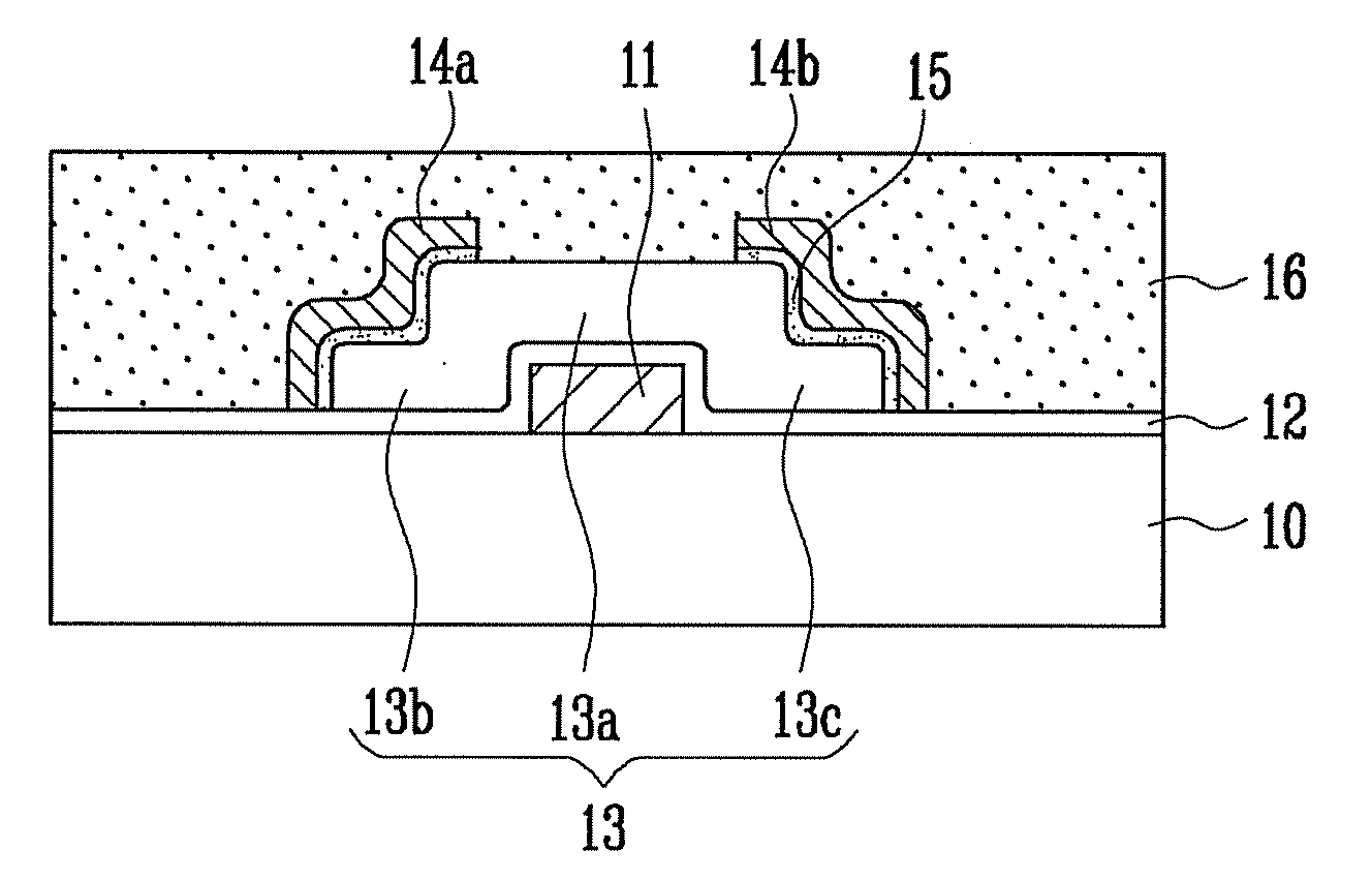
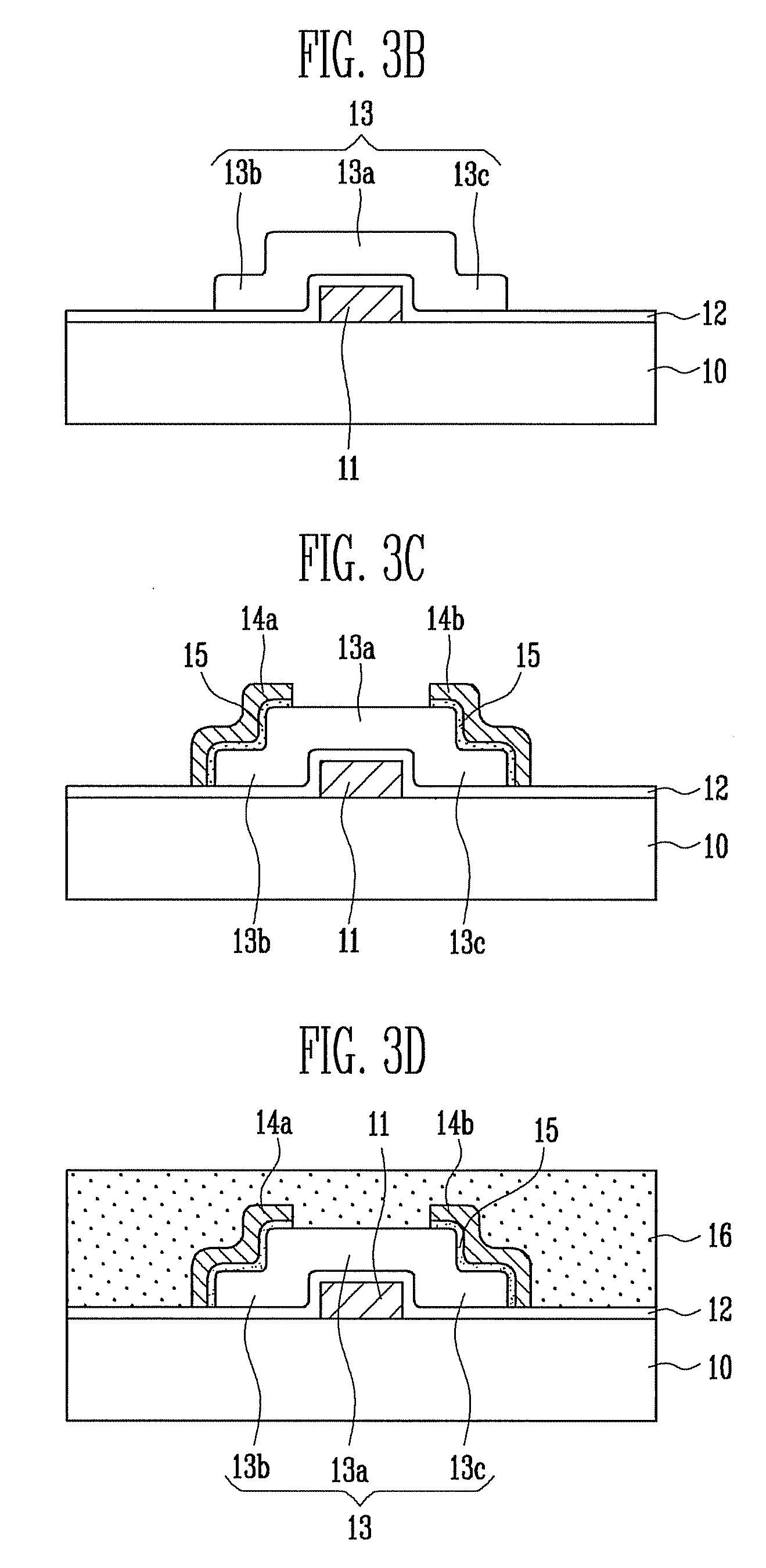
[0028]FIG. 1 is a cross-sectional view explaining a thin film transistor according to a first aspect of the present invention, wherein the thin film transistor having a bottom gate structure is ...


PUM


Abstract

A method of manufacturing a thin film transistor having a compound semiconductor with oxygen as a semiconductor layer and a method of manufacturing an organic light emitting display having the thin film transistor include: forming a gate electrode on an insulating substrate; forming a gate insulating layer on the gate electrode; forming a semiconductor layer including oxygen ions on the gate insulating layer, and including a channel region, a source region, and a drain region; forming a source electrode and a drain electrode to contact the semiconductor layer in the source region and the drain region, respectively; and forming a passivation layer on the semiconductor layer by coating an organic material, wherein a carrier density of the semiconductor layer is maintained in the range of 1E+17 to 1E+18 / cm3 to have stable electrical property.

Description

CROSS-REFERENCE TO RELATED APPLICATION[0001]This application claims the benefit of Korean Patent Application No. 2007-133508 filed on Dec. 18, 2007 in the Korean Intellectual Property Office, the entire content of which is incorporated herein by reference.BACKGROUND OF THE INVENTION[0002]1. Field of the Invention[0003]Aspects of the present invention relate to a method of manufacturing a thin film transistor and a method of manufacturing an organic light emitting display having the thin film transistor, and more particularly to a method of manufacturing a thin film transistor having a compound semiconductor containing oxygen as a semiconductor layer and a method of manufacturing an organic light emitting display having the thin film transistor.[0004]2. Description of the Related Art[0005]Generally, a thin film transistor includes a semiconductor layer including a channel region and source and drain regions, and a gate electrode formed on the channel region and electrically insulated...

Claims


Application Information

Patent Timeline
Patent Type & Authority Applications(United States)
IPC IPC(8): H01L21/336H01L51/40
CPCH01L29/7869H01L27/3244H10K59/12H01L29/06H01L27/1222H01L29/4908H01L29/41733H01L29/786H01L21/02565H01L27/1251H01L29/78618H10K59/1213
Inventor LEE, HUN-JUNGJEONG, JAE-KYEONGSHIN, HYUN-SOOJEONG, JONG-HANPARK, JIN-SEONGMO, STEVE Y.G.
Owner SAMSUNG DISPLAY CO LTD
Why Eureka
Try Eureka