Semiconductor device fabricating method and fabricating apparatus

Active Publication Date: 2009-06-18
TAIWAN SEMICON MFG CO LTD
View PDF2 Cites 9 Cited by
  • Summary
  • Abstract
  • Description
  • Claims
  • Application Information

AI Technical Summary

Benefits of technology

[0027]In accordance with the present invention, there is the effect that, in a case in which obverse electrodes of a semiconductor chip, at which

Problems solved by technology

However, a conventional bonding device does not suppose the conveying of a semiconductor chip with electrodes at both sides at which bump electrodes are formed at the obverse and the reverse.
Various problems have therefore arisen.
Due to the region where the obverse side bump electrode 32 is provided being sucked, the problem arises that the bump electrode 32 does not contact the bump electrode of the package substrate, and the opposing bump electrodes are n

Method used


Image

  • Semiconductor device fabricating method and fabricating apparatus
  • Semiconductor device fabricating method and fabricating apparatus
  • Semiconductor device fabricating method and fabricating apparatus

Examples


first exemplary embodiment

Bonding Device

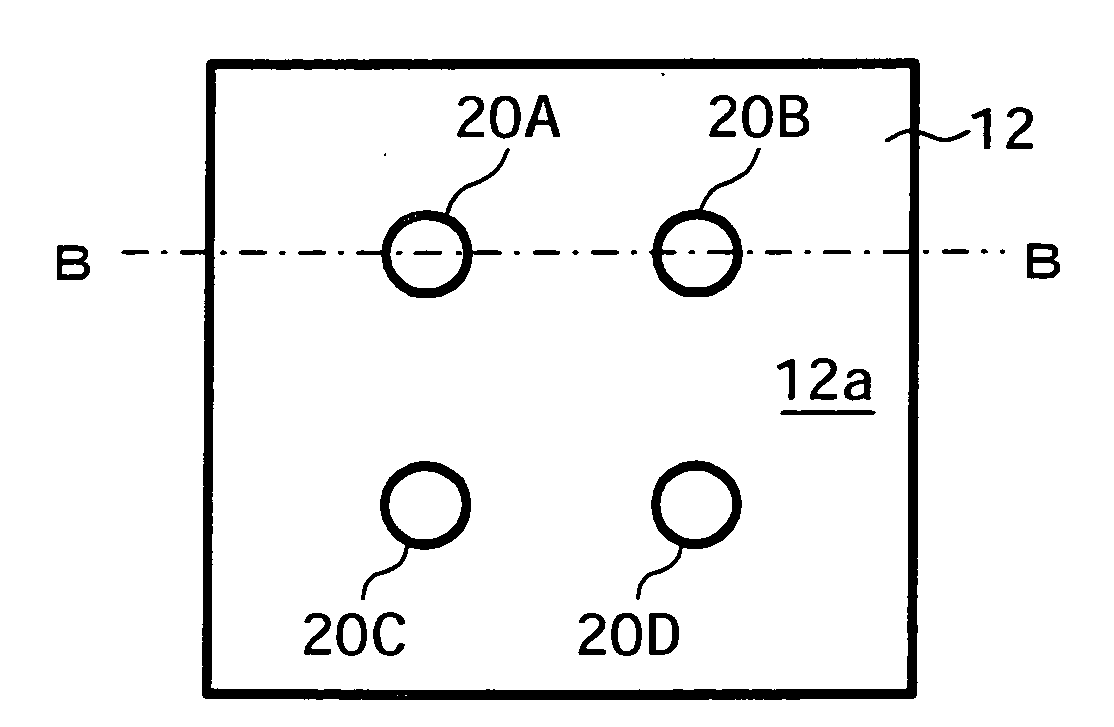
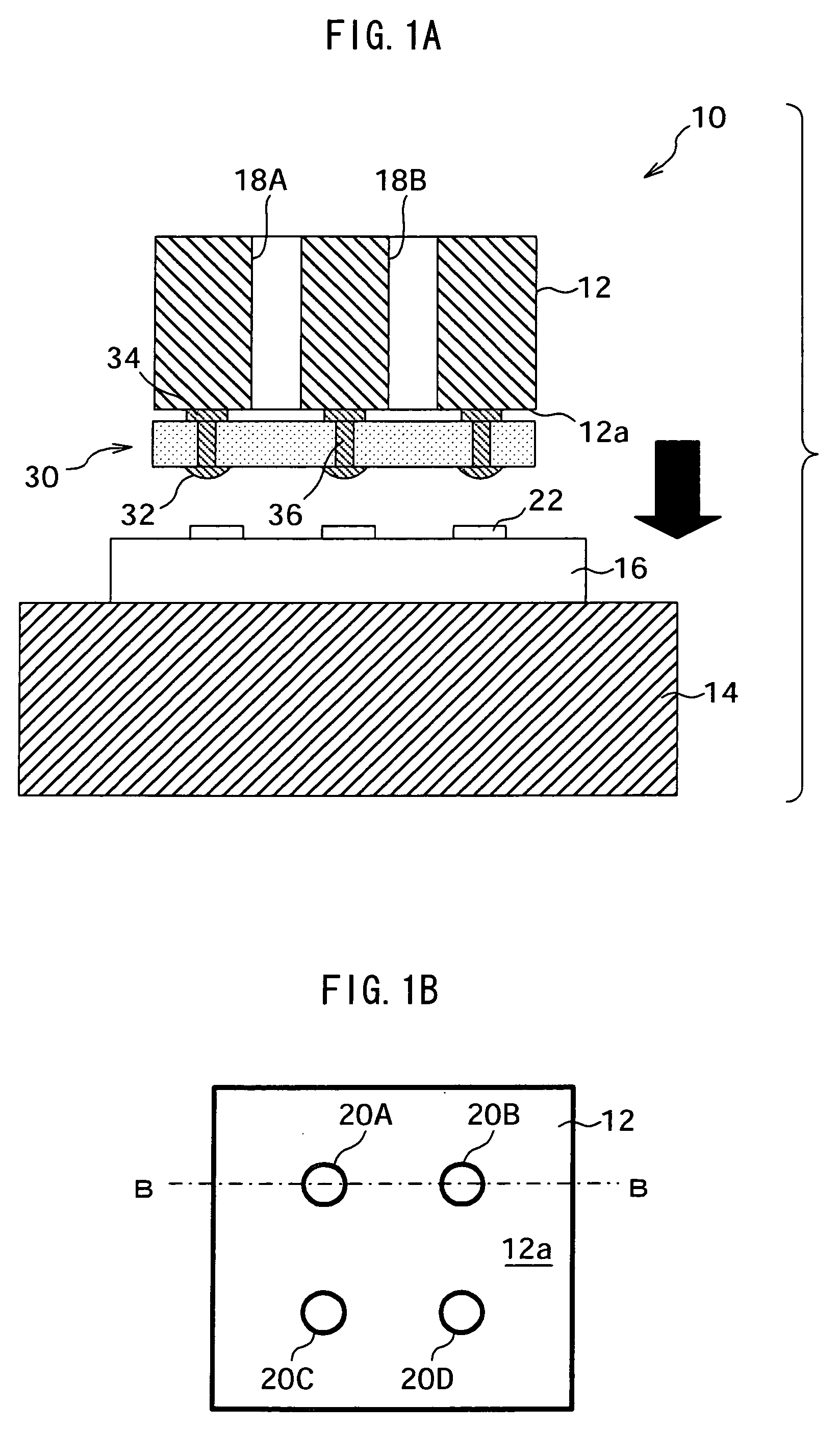
[0049]FIG. 1A is a schematic sectional view showing the structure of a bonding device relating to a first exemplary embodiment of a fabricating apparatus of the present invention. FIG. 1B is a plan view of an attracting surface of a bonding head. FIG. 1A corresponds to a cross-sectional view along line B-B of FIG. 1B. A bonding head 12, that is parallelepiped and supported movably, and a stage 14, that holds a package substrate 16 at which plural bump electrodes 22 serving as substrate electrodes are formed, are provided at a bonding device 10. The bonding head 12 is driven by an unillustrated driving device, and can move upward, downward, left and right within a predetermined range from the stage 14.

[0050]The bonding head 12 functions as a holding member that sucks and holds a semiconductor chip. Plural suction holes 18 that pass-through the bonding head 12 are provided at the bonding head 12. The plural suction holes 18 are connected to an unillustrated suction devic...

second exemplary embodiment

[0065]A bonding device relating to a second exemplary embodiment has a structure similar to that of the first exemplary embodiment, other than the structure of the bonding head. Therefore, description of the overall structure will be omitted, and only the structure of the bonding head will be described hereinafter. FIG. 5A is a plan view of an attracting surface of a bonding head, and FIG. 5B is a cross-sectional view along line D-D of FIG. 5A. Further, FIG. 5C is a drawing showing a layout of attracting openings that corresponds to the joining regions.

[0066]A bonding head 40 relating to the second exemplary embodiment has an attracting surface 40a that is rectangular in plan view. Plural suction holes 42 that pass-through the bonding head 40 are provided at the bonding head 40. Although only suction holes 42A, 42B are shown in the cross-sectional view of FIG. 5B, the bonding head 40 has the four suction holes 42A through 42D as shown in FIG. 5A. The suction holes 42A through 42D ar...

third exemplary embodiment

[0075]In the third exemplary embodiment, a bonding head is designed by assuming joining regions that are different than those in the first exemplary embodiment and the second exemplary embodiment. Further, a bonding device relating to the third exemplary embodiment has a structure similar to that of the first exemplary embodiment, other than the structure of the bonding head. Therefore, description of the overall structure will be omitted, and only the structure of the bonding head will be described hereinafter.

[0076]FIG. 6 is a plan view schematically showing joining regions at which the bump electrodes are joined to one another. The illustrated joining regions differ from the joining regions shown in FIG. 3B with regard to the point that a joining portion is not provided in the center of the matrix of five lines and five rows. A different layout of the attracting openings is possible when assuming the joining regions shown in FIG. 6 for a case in which the semiconductor chip 30 is...


PUM


Abstract

Respective attracting openings of a bonding head are disposed so as to avoid joining regions at which bump electrodes (obverse electrodes) of a semiconductor chip are joined with bump electrodes of a package substrate. Bump electrodes (reverse electrodes) that are connected to the bump electrodes are provided at a reverse side of the semiconductor chip at positions opposing the bump electrodes. Because the attracting openings do not overlap the joining regions, the bump electrodes (reverse electrodes) are not suctioned at the joining regions.

Description

CROSS-REFERENCE TO RELATED APPLICATION[0001]This application claims priority under 35 USC 119 from Japanese Patent Application No. 2007-322099, the disclosure of which is incorporated by reference herein.BACKGROUND OF THE INVENTION[0002]1. Field of the Invention[0003]The present invention relates to a semiconductor device fabricating method and fabricating apparatus. In particular, the present invention relates to a semiconductor device fabricating method and fabricating apparatus that include a process of picking-up and conveying a semiconductor chip, and flip-chip connecting obverse electrodes of the semiconductor chip to a package substrate.[0004]2. Description of the Related Art[0005]Semiconductor chips that have been separated into individual chips from a wafer are picked-up one-by-one and conveyed to a bonding device. Conventionally, when carrying out bonding by flip-chip connection, a bonding device having a bonding head that is generally called a collet is used. A single suc...

Claims


Application Information

Patent Timeline
IPC IPC(8): H01L23/48
CPCH01L24/75H01L2224/16H01L2224/75H01L2224/75301Y10T29/53178H01L2924/01005H01L2924/01006H01L2924/01033Y10T29/53961H01L2224/75745H01L2224/05573H01L2224/0615H01L2224/13025H01L2924/00014H01L2224/05599
Inventor SAEKI, YOSHIHIRO
Owner TAIWAN SEMICON MFG CO LTD
Why Eureka
Try Eureka