Method of correcting systematic error in a metrology system

Active Publication Date: 2009-06-18
TOKYO ELECTRON LTD
View PDF2 Cites 22 Cited by
  • Summary
  • Abstract
  • Description
  • Claims
  • Application Information

AI Technical Summary

Problems solved by technology

During a fabrication process, a drift in one or more process parameters can result in deviations on the device critical dimensions (CDs), potentially rendering the devices useless.
One is that the measurement process is destructive and the other is that it cannot be used in-situ, which prohibits its deployment in integrated metrology.
Measurements taken of the same sample on multiple scatterometry tools or optical metrology systems yield different scatterometry spectra, since each tool is prone to tool specif

Method used


Image

  • Method of correcting systematic error in a metrology system
  • Method of correcting systematic error in a metrology system
  • Method of correcting systematic error in a metrology system

Examples


Embodiment Construction

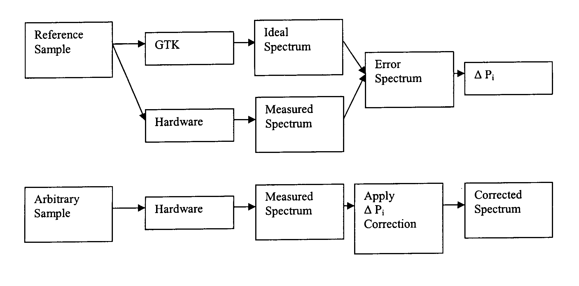
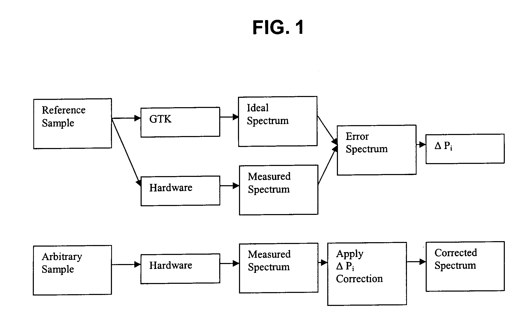
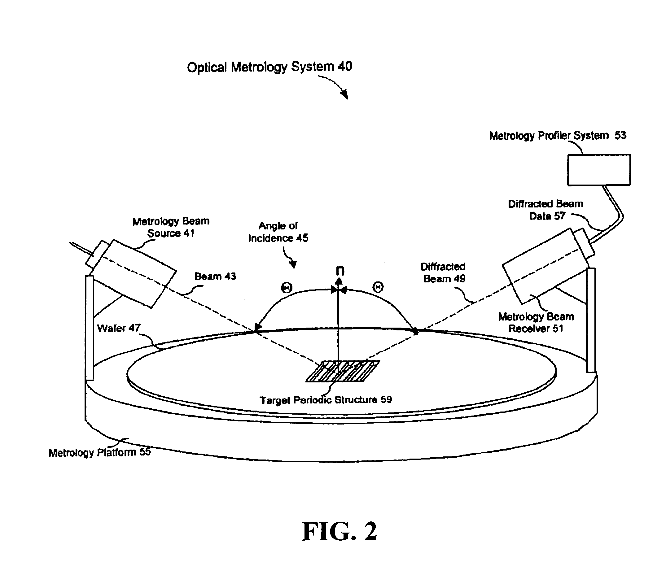
[0026]Methods for correcting systematic error in a metrology system is disclosed in various embodiments. However, one skilled in the relevant art will recognize that the various embodiments may be practiced without one or more of the specific details, or with other replacement and / or additional methods, materials, or components. In other instances, well-known structures, materials, or operations are not shown or described in detail to avoid obscuring aspects of various embodiments of the invention. Similarly, for purposes of explanation, specific numbers, materials, and configurations are set forth in order to provide a thorough understanding of the invention. Nevertheless, the invention may be practiced without specific details. Furthermore, it is understood that the various embodiments shown in the figures are illustrative representations and are not necessarily drawn to scale.

[0027]Reference throughout this specification to “one embodiment” or “an embodiment” means that a particu...


PUM


Abstract

A method for correcting systematic errors in an optical measurement tool in which a first diffraction spectrum is measured from a standard substrate including a layer having a known refractive index and a known extinction coefficient by exposing the standard substrate to a spectrum of electromagnetic energy. A tool-perfect diffraction spectrum is calculated for the standard substrate. A hardware systematic error is calculated by comparing the measured diffraction spectrum to the calculated tool-perfect diffraction spectrum. A second diffraction spectrum from a workpiece is measured by exposing the workpiece to the spectrum of electromagnetic energy, and the measured second diffraction spectrum is corrected based on the calculated hardware systematic error to obtain a corrected diffraction spectrum.

Description

CROSS REFERENCE TO RELATED APPLICATIONS[0001]This application is related to Attorney Docket No. 319002US entitled “Optical Measurement System with Systematic Error Correction” filed on ______ as U.S. Ser. No. ______.BACKGROUND OF THE INVENTION[0002]1. Field of the Invention[0003]The field of invention relates generally to optical measurement tools and, more particularly, to a method for correcting systematic error in such tools.[0004]2. Description of the Related Art[0005]Characteristics of semiconductor devices are directly dependent on the shapes and dimensions of one or more layers and / or features of a device. During a fabrication process, a drift in one or more process parameters can result in deviations on the device critical dimensions (CDs), potentially rendering the devices useless. Optical metrology has been traditionally employed to monitor semiconductor fabrication processes. Scanning Electron Microscopy (SEM) has been in the forefront in this area. Commonly referred to a...

Claims


Application Information

Patent Timeline
IPC IPC(8): G01B11/02
CPCG01B21/045
Inventor KAUSHAL, SANJEEVSANKARANARAYANAN, SAIRAMSUGISHIMA, KENJI
Owner TOKYO ELECTRON LTD
Why Eureka
Try Eureka