
Solid-state imaging device and camera

a solid-state imaging and camera technology, applied in the field of solid-state imaging devices and cameras, can solve the problems of large impact on the power consumption of the image sensor as a whole, insufficient improvement of the image sensor, so as to reduce power consumption, reduce power consumption, and improve image quality

Active Publication Date: 2009-06-25
PANASONIC SEMICON SOLUTIONS CO LTD
View PDF11 Cites 20 Cited by
  • Summary
  • Abstract
  • Description
  • Claims
  • Application Information

AI Technical Summary

Benefits of technology

[0023]The object of the present invention is therefore to provide a solid-state imaging device and a camera that can change gain when necessary, and reduce power consumption more than those of conventional techniques.

Problems solved by technology

However, the construction of the image sensor according to the conventional technique 2 is not fully satisfactory in terms of reducing the power consumption of the image sensor as a whole.
Consequently, the power consumption of the column A / D circuit 25 alone has a large impact on the power consumption of the image sensor as a whole.

Method used


Image

  • Solid-state imaging device and camera
  • Solid-state imaging device and camera
  • Solid-state imaging device and camera

Examples


first embodiment

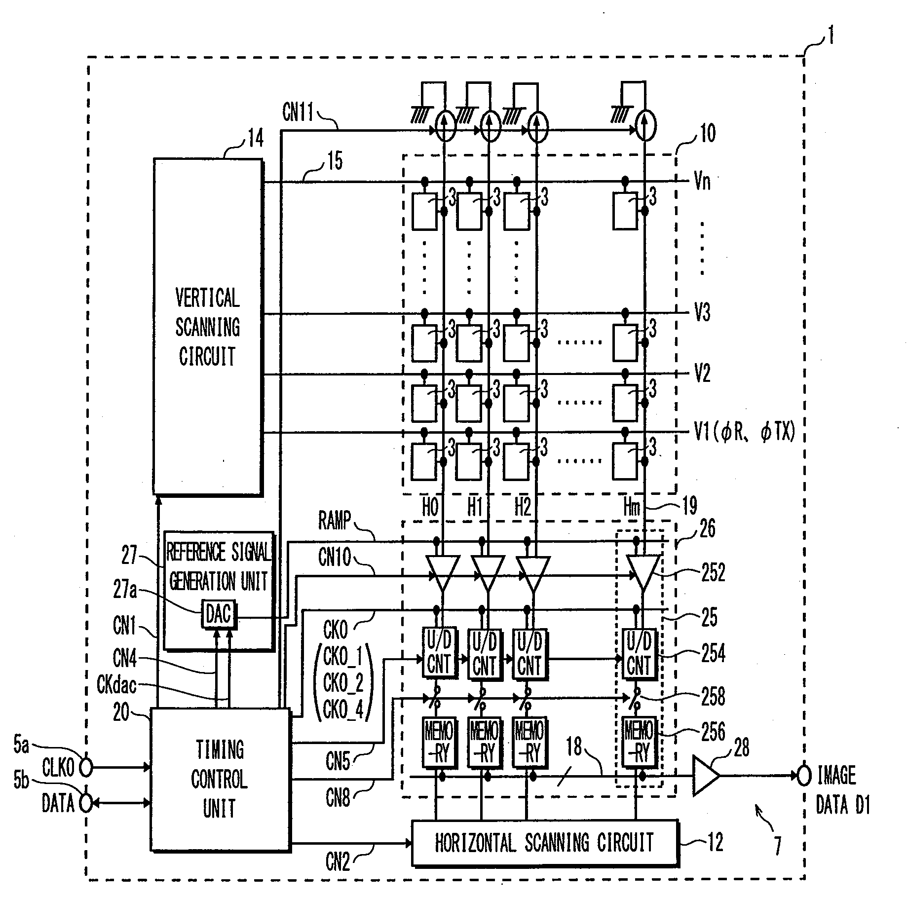
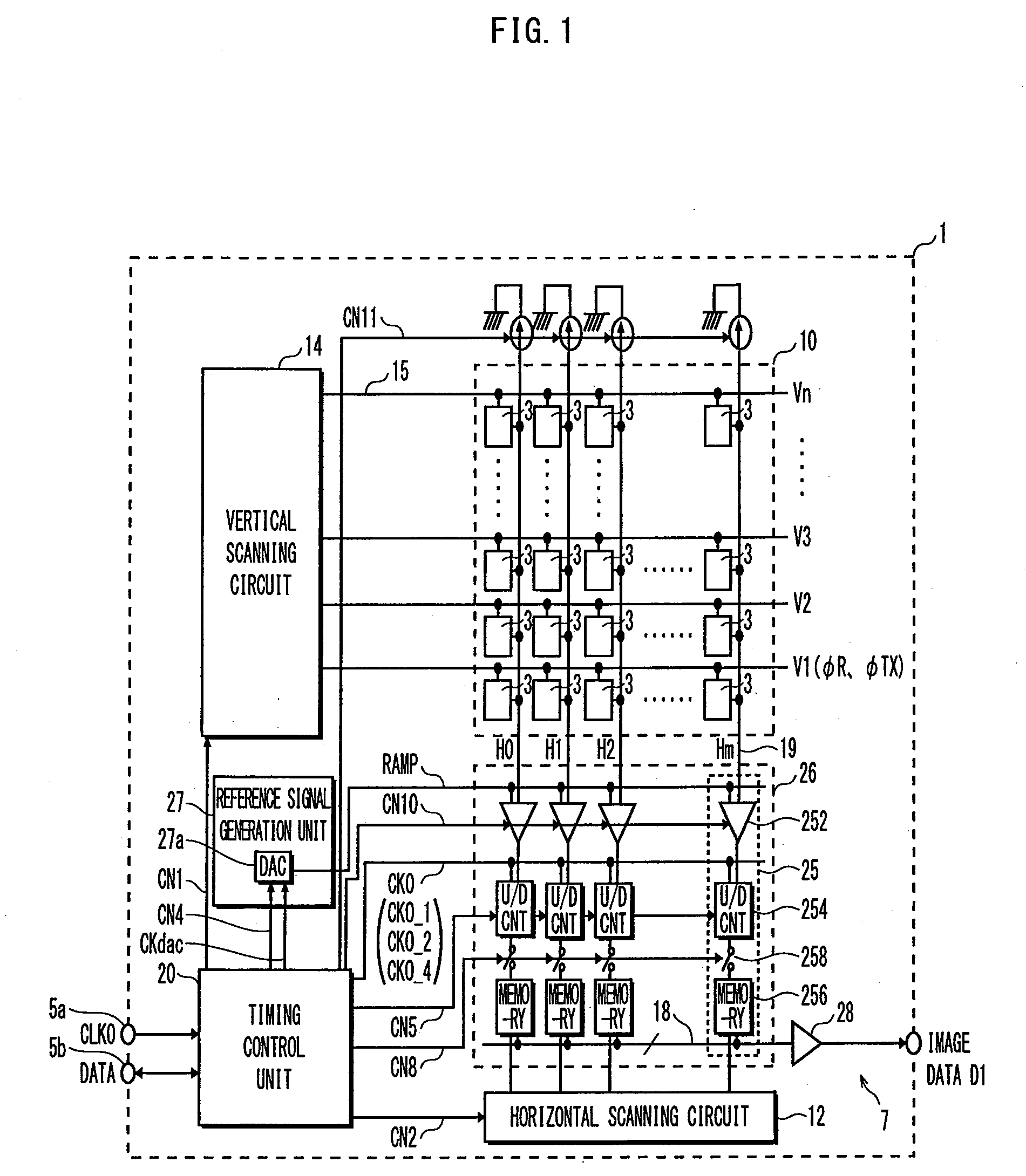
[0059]FIG. 1 is a schematic construction diagram showing an image sensor according to a first embodiment of the present invention.

[0060]The difference between an image sensor according to the first embodiment of the present invention and an image sensor according to a conventional technique (shown in FIG. 17) is mainly the construction of a timing control unit. This causes a difference in (i) a clock CKdac that is input into a reference signal generation unit 27 and (ii) a clock CK0 that is input into a column A / D circuit 25. In other words, a timing control unit 20 according to the first embodiment fixes the frequency of the clock CKdac based on which reference signals are generated, and changes the frequency of a clock CK0 when necessary (CK0_1, CK0_2, CK0_4), where counts are made based on the clock CK0. In contrast, a timing control unit 40 according to a conventional technique (conventional technique 2) changes the frequency of the clock CKdac when necessary (CKdac 1, CKdac 2, ...

second embodiment

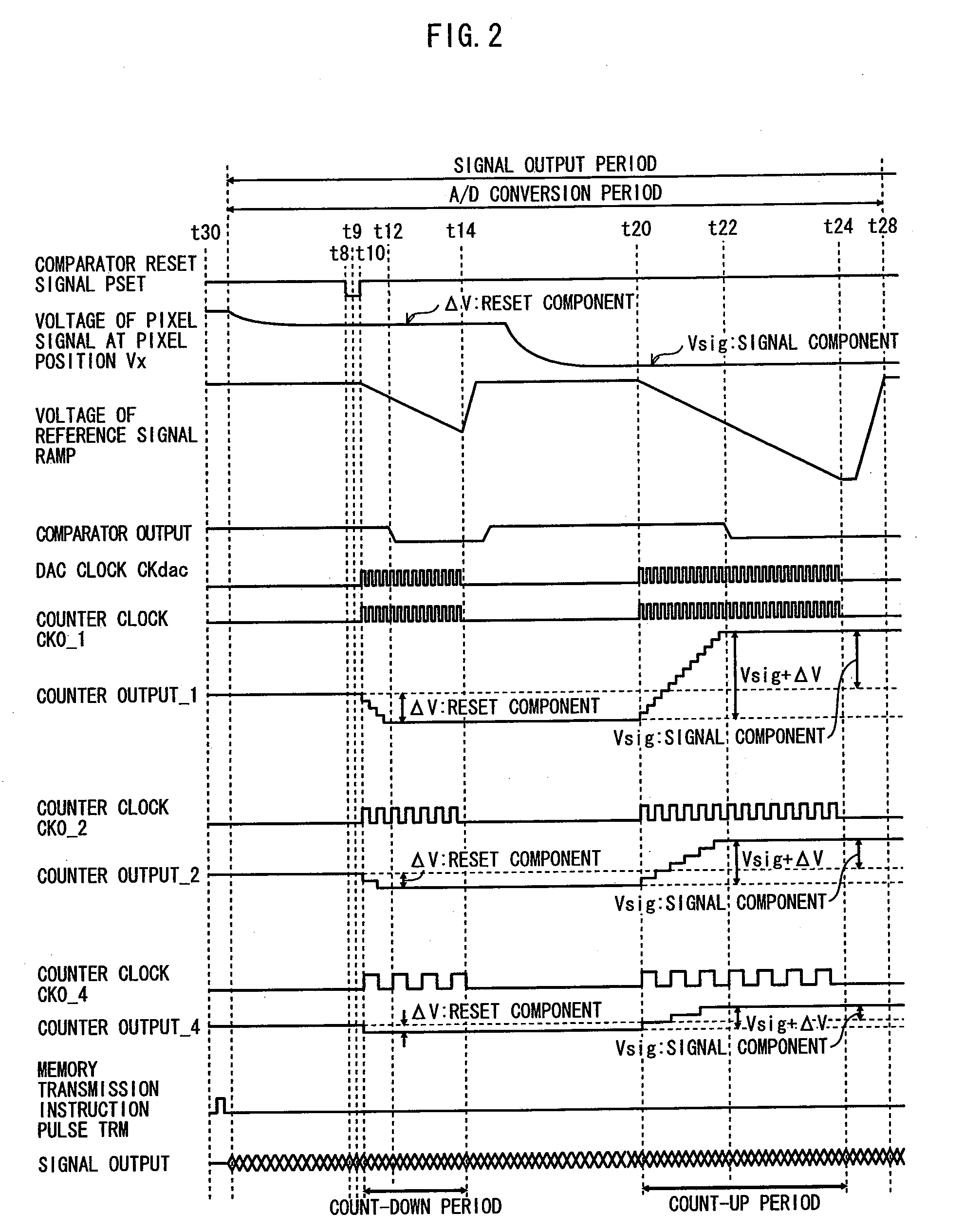
[0080]The following describes the operation of an image sensor according to a second embodiment of the present invention, particularly the operation when an pixel signal is A / D converted by the column A / D circuit 25. Note that the description of a schematic construction of the image sensor is omitted, since the construction is the same as that shown in FIG. 1.

[0081]FIG. 6 is a timing chart showing the operation of the image sensor according to the second embodiment of the present invention.

[0082]The second embodiment is the same as the first embodiment in that (i) the clock CKdac is input into the reference signal generation unit 27 and (ii) one of the clock CK0_1, the clock CK0_2, and the clock CK0_4 is selectively input into the column A / D circuit 25.

[0083]However, an upper limit of the number of counts, for each of the clock CK0_1, the clock CK0_2, and the clock CK0_4, is fixed in the second embodiment, which is different from the first embodiment. In other words, the higher the ...


PUM


Abstract

A solid-state imaging device comprises a pixel array; a reference signal generation unit operable to generate a reference signal that changes monotonically for a predetermined period in a horizontal period; a comparator operable to compare the level of a pixel signal with the level of a reference signal; a counter operable to count input clock pulses; a memory operable to store the number of counts counted by the counter as a digital value; and a timing control unit operable to generate a clock that is to be input into the counter, and change frequency of the clock that is to be input into the counter based on external input data.

Description

BACKGROUND OF THE INVENTION[0001](1) Field of the Invention[0002]The present invention relates to a solid-state imaging device and a camera, and in particular to a MOS type solid-state imaging device such as a CMOS image sensor.[0003](2) Description of the Related Art[0004]In recent years, various methods have been suggested for reading signals in a CMOS image sensor. Generally speaking, commonly used are CMOS image sensors of a column parallel output type in which a row of pixels is selected in a pixel array. Then, pixel signals generated in the selected pixels are read in parallel via a vertical signal line (also referred to as a column signal line). An image sensor that has also been suggested is of a column A / D type, which is provided with an A / D conversion circuit for each vertical signal line, so that a pixel signal is converted from analog to digital form inside the CMOS image sensor.[0005]FIG. 15 is a schematic construction diagram of an image sensor shown in Japanese laid-o...

Claims


Application Information

Patent Timeline
Patent Type & Authority Applications(United States)
IPC IPC(8): H01L27/00H04N25/00
CPCH03M1/1023H04N5/3742H03M1/56H03M1/1295H03M1/123H03M1/18H04N25/767H04N25/78
Inventor MURAKAMI, MASASHISHIMOMURA, KENICHI
Owner PANASONIC SEMICON SOLUTIONS CO LTD
Learn More