Light emitting diode element and method for fabricating the same

a technology of light-emitting diodes and diodes, which is applied in the direction of semiconductor/solid-state device manufacturing, electrical equipment, semiconductor devices, etc., can solve the problems of reduced probability that light leaves a semiconductor, photons can only be totally reflected inside a chip, and led usually has insufficient light efficiency, so as to reduce the probability of total internal reflection and reduce the cost. , the effect of promoting the light extraction efficiency of led

Active Publication Date: 2009-06-25
TEKCORE CO LTD
View PDF12 Cites 239 Cited by
  • Summary
  • Abstract
  • Description
  • Claims
  • Application Information

AI Technical Summary

Benefits of technology

[0014]The present invention is superior in being a multi-incline LED, which is formed via etching a substrate to obtain basins having inclined natural crystal planes and selectively growing LED epitaxial layers inside the basins. Via multiple inclines, the probability of total internal reflection is reduced, and the light extraction efficiency of LED is promoted. Further, the simple fabrication process of the present invention is favorable for mass production and can reduce the cost.

Problems solved by technology

Besides, the parallel faces of a parallelepiped decrease the probability that light leaves a semiconductor from an interface.
Thus, photons can only be totally reflected inside a chip until they are completely absorbed and converted into heat.
Therefore, LED usually has insufficient light efficiency.
However, the technology of TIP LED can only apply to red light AlGaInP / GaP LED chips.
A gallium nitride (GaN) LED is epitaxially grown on a sapphire substrate, which is very hard to mechanically fabricate.
Therefore, the TIP LED technology cannot apply to GaN LED.
Therefore, this technology is hard to commercialize.
However, it has the disadvantages of needing two epitaxial processes, which make LED fabrication more complicated.

Method used


Image

  • Light emitting diode element and method for fabricating the same
  • Light emitting diode element and method for fabricating the same
  • Light emitting diode element and method for fabricating the same

Examples


Embodiment Construction

[0020]The technical contents of the present invention are to be described in detail with embodiments. However, these embodiments are only to demonstrate the present invention but not to limit the scope of the present invention.

[0021]The present invention utilizes an etching technology to form basins with inclined natural crystal planes on a substrate. Epitaxial layers of LED are selectively grown in the basins to form an LED with several inclined planes. Thereby, a high light-extraction efficiency LED is achieved.

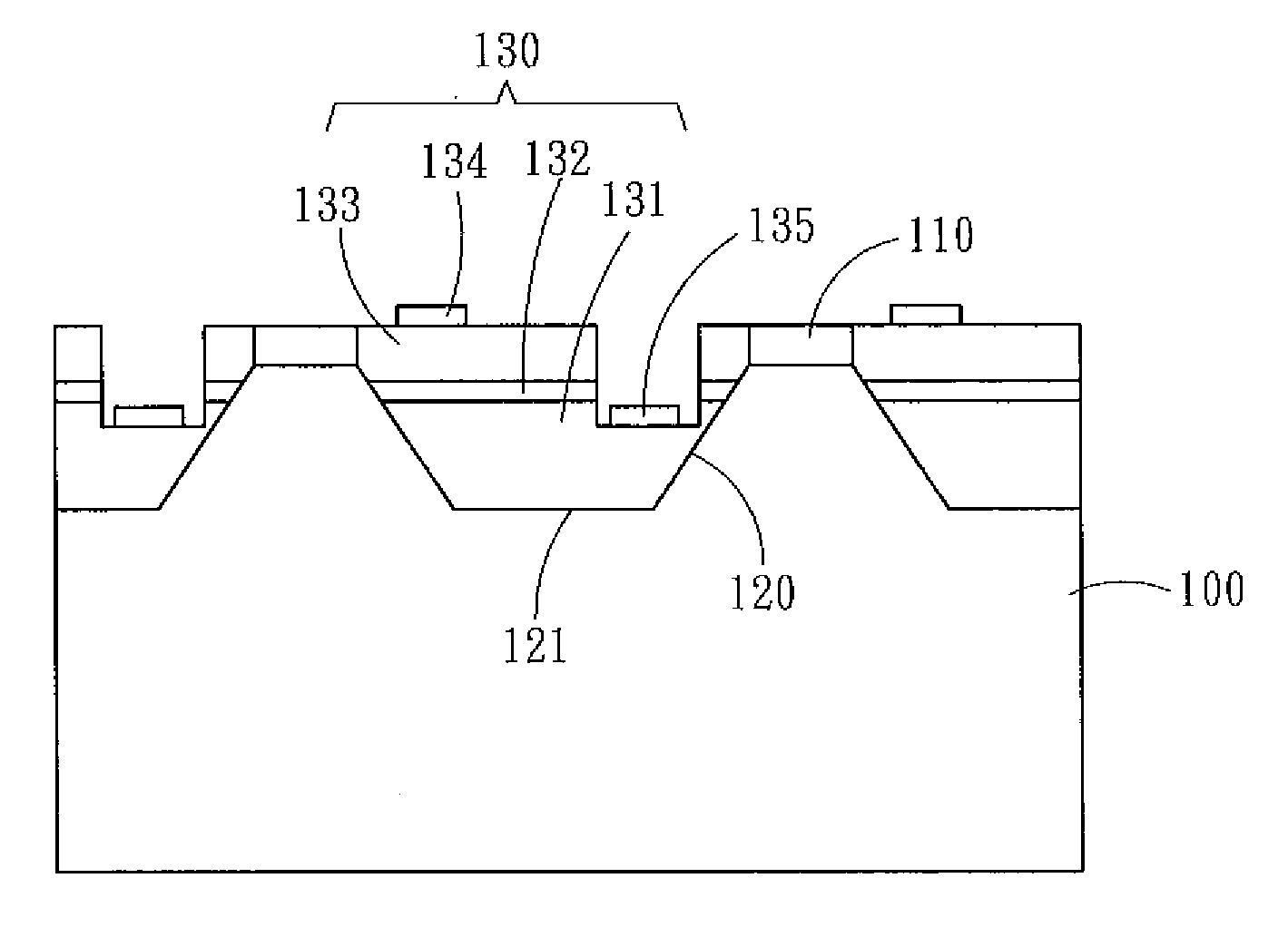
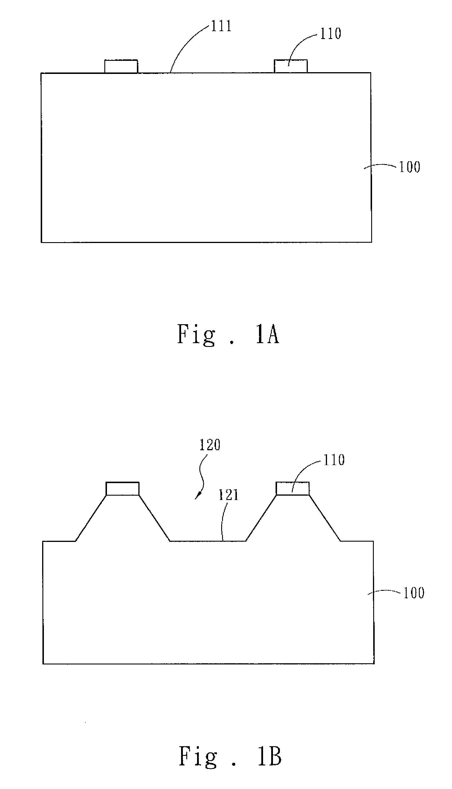
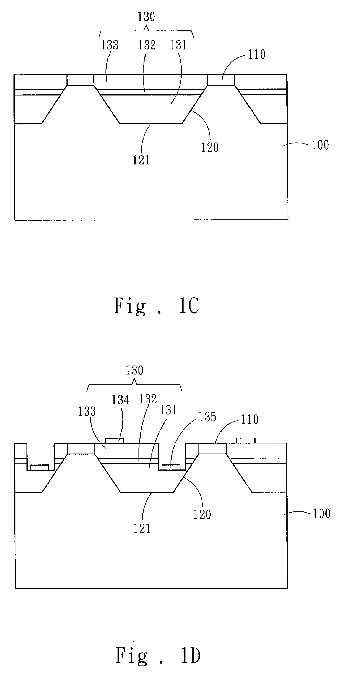
[0022]Refer to from FIG. 1A to FIG. 1E diagrams schematically showing the process of a method according to the present invention. The method of the present invention comprises the following steps:[0023](a) providing a substrate 100, forming a passivation layer 110 on the substrate 100 and defining a plurality of polygonal etch areas 111, as shown in FIG. 1A, wherein the substrate 100 may be made of sapphire, silicon carbide (SiC), silicon (Si), gallium arsenide (GaAs) or al...


PUM


Abstract

The present invention discloses a light emitting diode (LED) element and a method for fabricating the same, which can promote light extraction efficiency of LED, wherein a substrate is etched to obtain basins with inclined natural crystal planes, and an LED epitaxial structure is selectively formed inside the basin. Thereby, an LED element having several inclines is obtained. Via the inclines, the probability of total internal reflection is reduced, and the light extraction efficiency of LED is promoted.

Description

FIELD OF THE INVENTION[0001]The present invention relates to a light emitting diode element and a method for fabricating the same, particularly to a high light-extraction efficiency light emitting diode element and a method for fabricating the same.BACKGROUND OF THE INVENTION[0002]Traditionally, a light emitting diode (LED) is fabricated into a parallelepiped shape. An LED usually has a small total reflection critical angle because there is a great difference between the refractive indexes of a semiconductor and a packaging material. The light generated by LED reaching an interface by an angle greater than the total reflection critical angle will be totally reflected back to the interior of the LED chip. Besides, the parallel faces of a parallelepiped decrease the probability that light leaves a semiconductor from an interface. Thus, photons can only be totally reflected inside a chip until they are completely absorbed and converted into heat. Therefore, LED usually has insufficient...

Claims


Application Information

Patent Timeline
Patent Type & Authority Applications(United States)
IPC IPC(8): H01L33/00H01L33/10H01L33/20
CPCH01L33/20H01L33/10
Inventor LIN, HUNG-CHENGLEE, CHIA-MINGCHYI, JEN-INN
Owner TEKCORE CO LTD
Why Eureka
Try Eureka