Light-receiving element and display device
- Summary
- Abstract
- Description
- Claims
- Application Information
AI Technical Summary
Benefits of technology
Problems solved by technology
Method used
Image

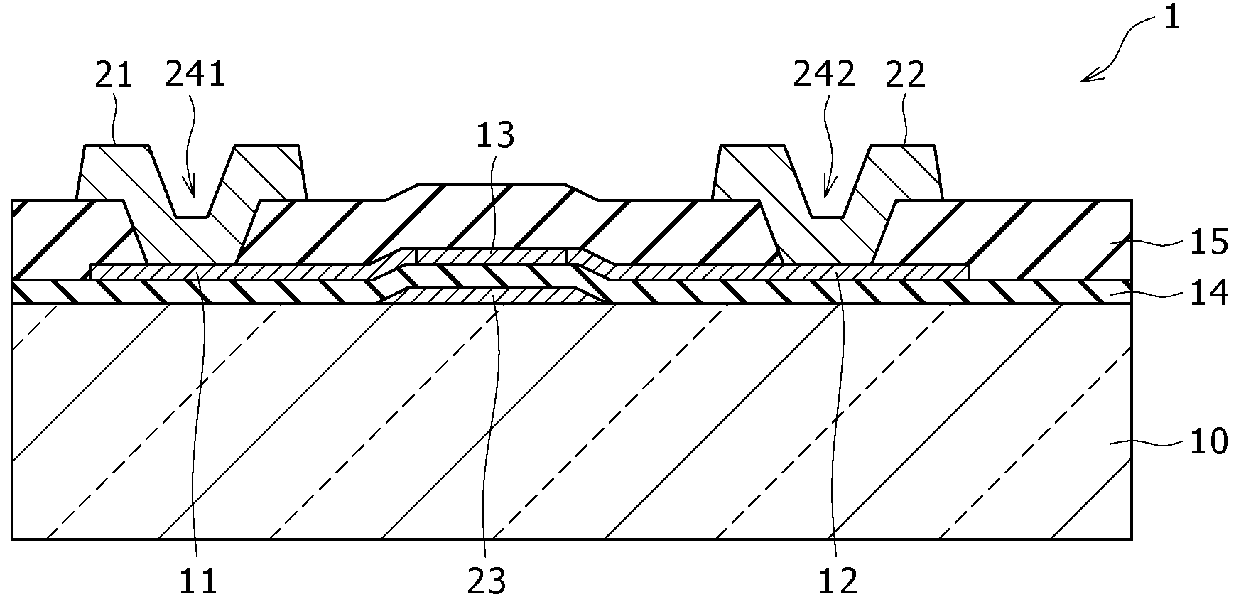
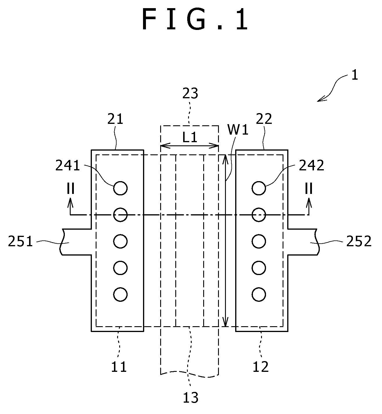
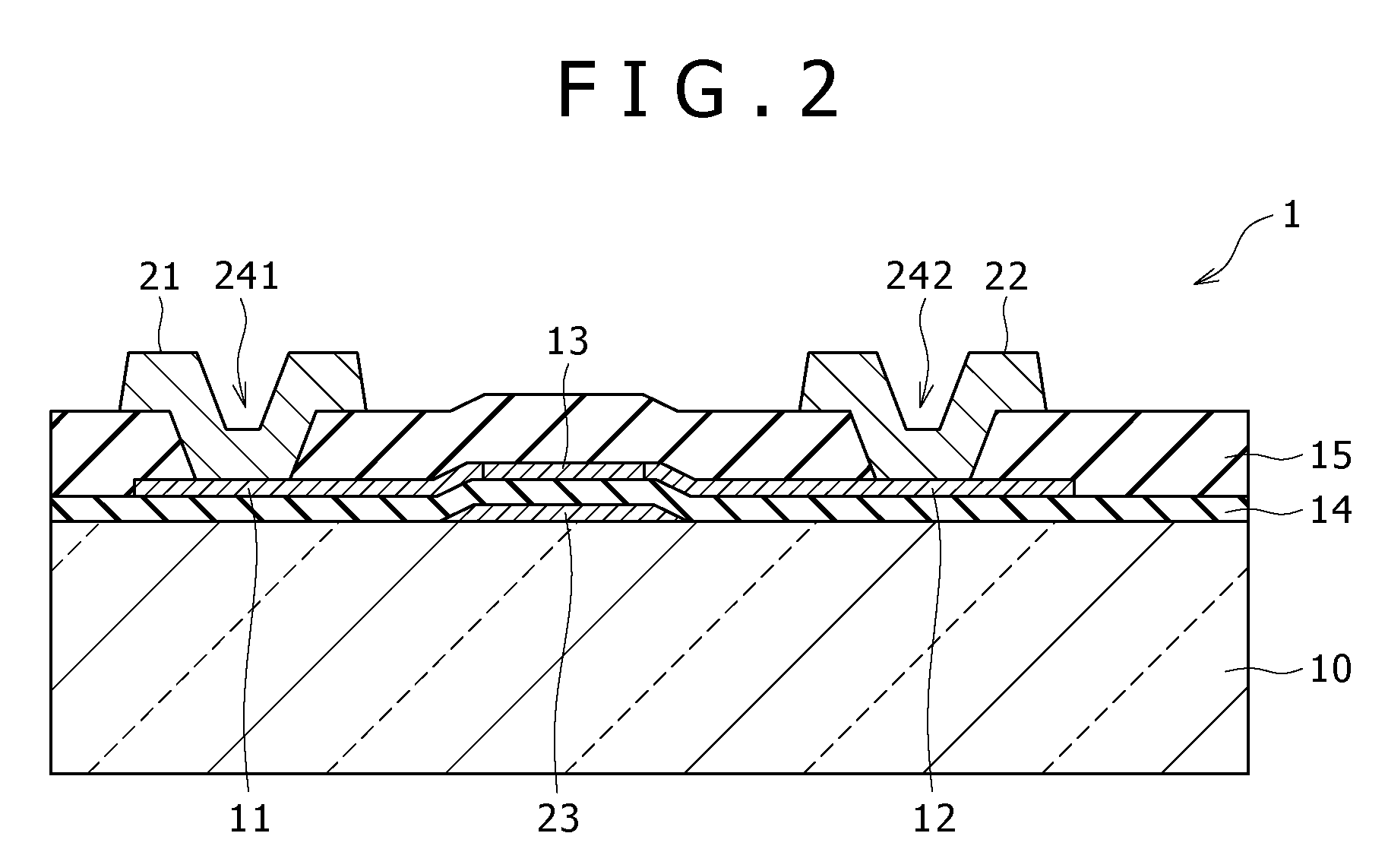
Examples
modification examples
[0071]Modification examples of the embodiment of the present invention will be described below. The same component in the modification examples as that in the above-described embodiment is given the same numeral, and the description thereof is omitted.
first modification example
[0072]FIG. 9 shows the planar structure of a light-receiving element (light-receiving element 1A) according to a first modification example. FIG. 10 shows the sectional structure of the light-receiving element 1A along line IV-IV in FIG. 9. In the light-receiving element 1A, the conductivity type of the impurity (p-type impurity) in a light-receiving part 13A is the p-type, and the voltage applied to the gate electrode 23 is positive potential. That is, the light-receiving part 13A is a p− layer.
[0073]Also in the light-receiving element 1A of the present modification example having such a configuration, generation of photocurrent can be facilitated and the light-reception sensitivity can be sufficiently enhanced due to the same operation as that of the above-described embodiment.
second modification example
[0074]FIG. 11 shows the sectional structure of a light-receiving element (light-receiving element 1B) according to a second modification example. The above-described embodiment and the first modification example relate to a bottom-gate light-receiving element in which the gate electrode 23 is formed under the p+ layer 11, the n+ layer 12, and the light-receiving part 13. In contrast, the light-receiving element 1B is a top-gate light-receiving element in which a gate electrode 23B is formed over the p+ layer 11, the n+ layer 12, and the light-receiving part 13. In the light-receiving element 1B, interlayer insulating films 161 and 162 and a gate insulating film 14B are formed.
[0075]Also in the light-receiving element 1B, the voltage applied to the gate electrode 23B is positive potential if the conductivity type of the impurity (p-type impurity) in the light-receiving part 13 is the p-type. On the other hand, the voltage applied to the gate electrode 23B is negative potential if the...
PUM
 Abstract
Description
Claims
Application Information
 - Generate Ideas
- Intellectual Property
- Life Sciences
- Materials
- Tech Scout
- Unparalleled Data Quality
- Higher Quality Content
- 60% Fewer Hallucinations
Browse by: Latest US Patents, China's latest patents, Technical Efficacy Thesaurus, Application Domain, Technology Topic, Popular Technical Reports.
© 2025 PatSnap. All rights reserved.Legal|Privacy policy|Modern Slavery Act Transparency Statement|Sitemap|About US| Contact US: help@patsnap.com