Flip-chip type semiconductor light-emitting device, method for manufacturing flip-chip type semiconductor light-emitting device, printed circuit board for flip-chip type semiconductor light-emitting device, mounting structure for flip-chip type semiconductor light-emitting device, and light-emitting diode lamp

a technology of semiconductor light-emitting devices and flip-chip type semiconductors, which is applied in the direction of light-emitting diodes, lighting and heating devices, soldering devices, etc., can solve the problems of re-flow process, and achieve the effect of improving the finish of the soldering film and manufacturing the light-emitting devi

Active Publication Date: 2009-06-25
TOYODA GOSEI CO LTD
View PDF5 Cites 64 Cited by
  • Summary
  • Abstract
  • Description
  • Claims
  • Application Information

AI Technical Summary

Benefits of technology

[0050]According to the flip-chip type semiconductor light-emitting device (light-emitting device) of the present invention, since each of the electrode pads fixed to a positive electrode and a negative electrode is formed in the same shape, in a re-flow process for mounting a light-emitting device on a printed circuit board, there is no concern that the light-emitting device may be drawn to one bonding pad side, while it is floated, even when the light-emitting device is kept floated on liquefied solder, thereby making it possible to bond the light-emitting device with the printed circuit board at a target site in design accurately. More specifically, since each of the electrode pads is formed in the same shape, the self alignment effect is provided on flip-chip connection, thereby making it possible to bond the light-emitting device at a target site accurately.
[0051]Furthermore, according to a method for manufacturing the light-emitting device of the present invention, each of the electrode pads fixed to a positive electrode and a negative electrode can be formed in the same shape, thereby making it possible to manufacture easily the light-emitting d

Problems solved by technology

Furthermore, since the above-described soldering paste is difficult to coat on the electrodes 104 and 105 of the light-emitting

Method used


Image

  • Flip-chip type semiconductor light-emitting device, method for manufacturing flip-chip type semiconductor light-emitting device, printed circuit board for flip-chip type semiconductor light-emitting device, mounting structure for flip-chip type semiconductor light-emitting device, and light-emitting diode lamp
  • Flip-chip type semiconductor light-emitting device, method for manufacturing flip-chip type semiconductor light-emitting device, printed circuit board for flip-chip type semiconductor light-emitting device, mounting structure for flip-chip type semiconductor light-emitting device, and light-emitting diode lamp
  • Flip-chip type semiconductor light-emitting device, method for manufacturing flip-chip type semiconductor light-emitting device, printed circuit board for flip-chip type semiconductor light-emitting device, mounting structure for flip-chip type semiconductor light-emitting device, and light-emitting diode lamp

Examples


first embodiment

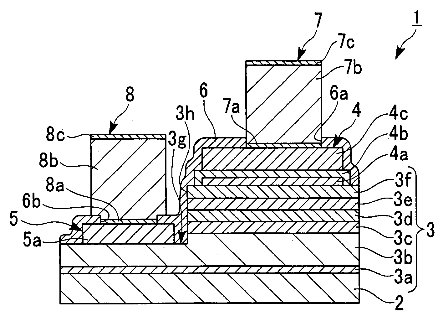
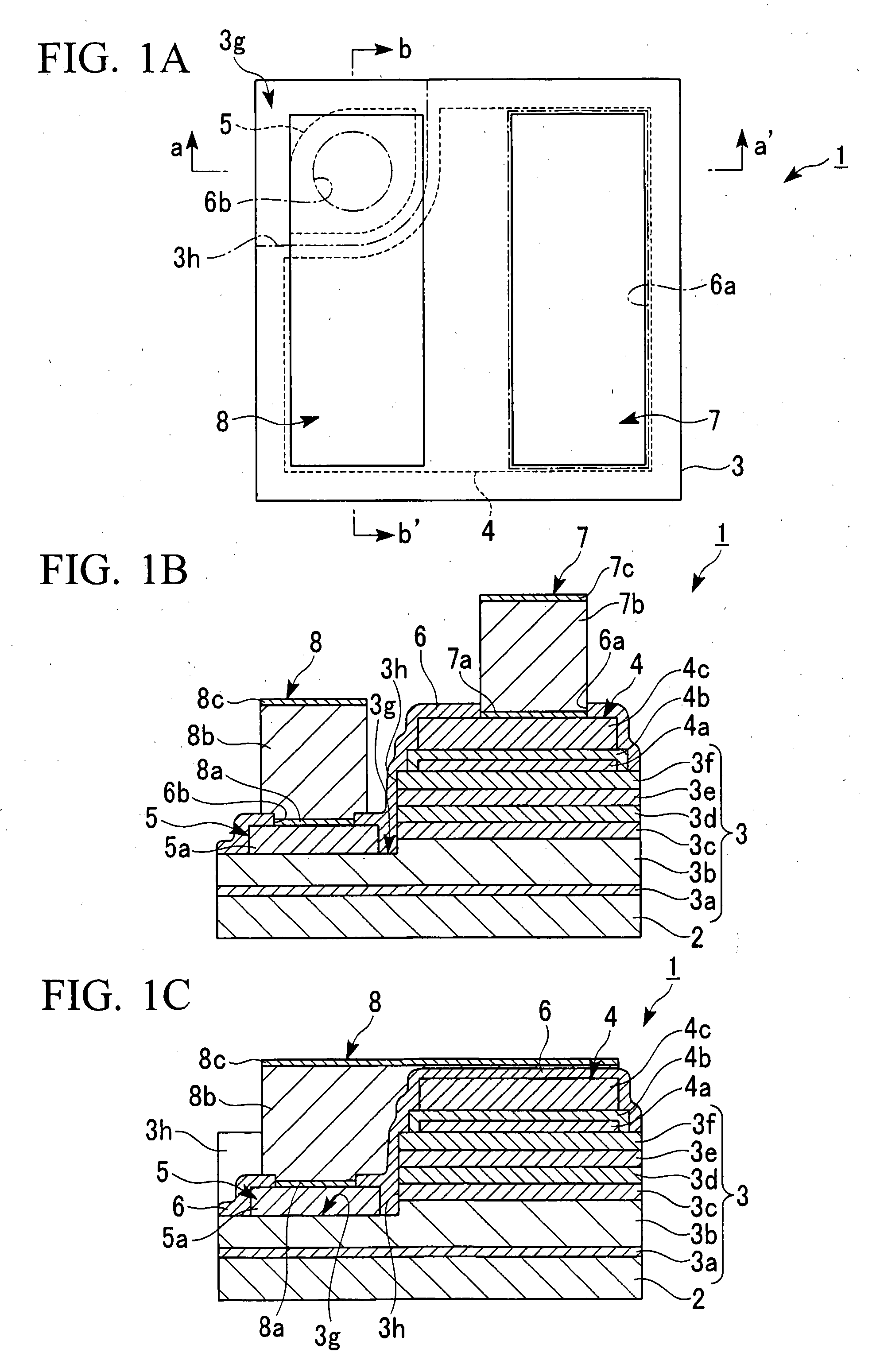
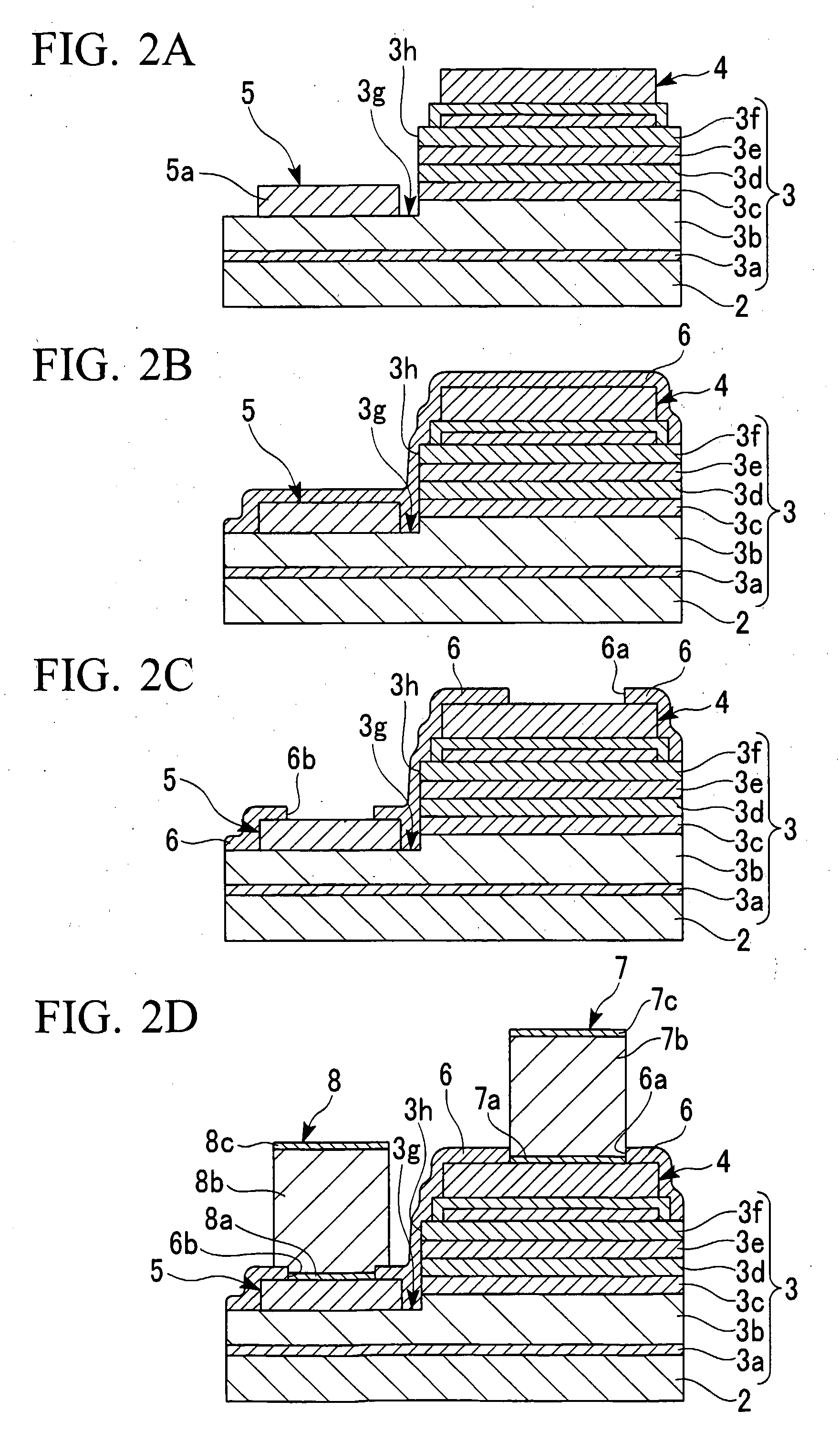
[0106]FIG. 1A is a bottom view showing the flip-chip type semiconductor light-emitting device of the present embodiment, FIG. 1B is a sectional pattern diagram corresponding to the line a-a′ of FIG. 1A, and FIG. 1C is a sectional pattern diagram corresponding to the line b-b′ of FIG. 1A.

[0107]As illustrated from FIG. 1A to FIG. 1C, a flip-chip type semiconductor light-emitting device 1 of the present embodiment (hereinafter referred to as light-emitting device 1) is called a gallium nitride type semiconductor light-emitting device, which is approximately rectangular when viewed from above, and constituted substantially of a transparent substrate 2 approximately rectangular when viewed from above, a semiconductor layer 3 approximately rectangular when viewed from above and stacked on the transparent substrate 2, a positive electrode 4 and a negative electrode 5 formed on the side opposite the transparent substrate 2 side of the semiconductor layer 3, a short-circuit preventing insula...

second embodiment

[0158]Next, a description will be given of a flip-chip type semiconductor light-emitting device which is a second embodiment of the present invention by referring to the drawings. FIG. 4A is a bottom view showing the flip-chip type semiconductor light-emitting device of the present embodiment, FIG. 4B is a sectional pattern diagram corresponding to the line c-c′ of the FIG. 4A. It should be noted that of constituent features of the light-emitting device given in FIG. 4, the same constituent features as those of the light-emitting device 1 of the first embodiment given in FIG. 1 are given the same symbols or numerals as those given in FIG. 1 and a description will be given of briefly or omitted.

[0159]The light-emitting device of the present embodiment is different from the light-emitting device 1 of the first embodiment given in FIG. 1 in that the short-circuit preventing insulator film is different in the forming region.

[0160]That is, as shown in FIG. 4, the light-emitting device 21...

third embodiment

[0172]Next, a description will be given of a third embodiment of the present invention by referring to the drawings. FIG. 5A is a bottom view showing the flip-chip type semiconductor light-emitting device of the present embodiment. FIG. 5B is a sectional pattern diagram corresponding to the line d-d′ of FIG. 5A, FIG. 5C is a sectional pattern diagram corresponding to the line e-e′ of FIG. 5A, and FIG. 5D is a sectional pattern diagram corresponding to the line f-f′ of FIG. 5A.

[0173]As shown in FIG. 5A to FIG. 5D, the flip-chip type semiconductor light-emitting device 31 (hereinafter referred to as light-emitting device 31) of the present embodiment is called a gallium nitride type semiconductor light-emitting device which is approximately in a rectangular shape when viewed from above. It is substantially constituted of a transparent substrate 32 approximately rectangular when viewed from above, a semiconductor layer 33 approximately rectangular when viewed from above and stacked on ...


PUM

PropertyMeasurementUnit
Widthaaaaaaaaaa
Shapeaaaaaaaaaa

Abstract

A flip-chip type semiconductor light-emitting device having a positive electrode and a negative electrode similar in electrode area and capable of preventing the misalignment of the light-emitting device by utilizing the self alignment effect in manufacturing a light-emitting diode lamp and a printed circuit board for the flip-chip type semiconductor light-emitting device are provided. Furthermore, adopted are a flip-chip type semiconductor light-emitting device 1 which is provided with a negative electrode pad and a positive electrode pad formed on the side opposite the transparent substrate side of the semiconductor layer, wherein each of the electrode pads is formed in the same shape as each other and a printed circuit board for the light-emitting device has a pair of the electrode patterns which are formed in the same shape as each other. Still furthermore, a soldering film is included in each of the electrode pads.

Description

CROSS REFERENCE TO RELATED APPLICATIONS[0001]Priority is claimed on Japanese Patent Application No. 2005-364338, filed Dec. 19, 2005, Japanese Patent Application No. 2006-090728, filed Mar. 29, 2006, and Japanese Patent Application No. 2006-116627, filed Apr. 20, 2006. This application is an application filed under 35 U.S.C. §111(a) claiming pursuant to 35 U.S.C. §119(e) of the filing date of Provisional Application 60 / 753,392 on Dec. 27, 2005, pursuant to 35 U.S.C. §111(b).TECHNICAL FIELD[0002]The present invention relates to a flip-chip type semiconductor light-emitting device, a method for manufacturing the flip-chip type semiconductor light-emitting device, a printed circuit board for the flip-chip type semiconductor light-emitting device, a mounting structure for the flip-chip type semiconductor light-emitting device and a light-emitting diode lamp, and in particular relates to technologies for preventing misalignment in mounting the flip-chip type semiconductor light-emitting ...

Claims


Application Information

Patent Timeline
IPC IPC(8): H01L33/00B23K1/20F21V21/00H01L33/38H01L33/48
CPCF21K9/00H01L33/08H01L33/20H01L2224/16H01L33/486H01L2933/0016H01L33/38
Inventor YASUDA, TAKAKITOMOZAWA, HIDEKI
Owner TOYODA GOSEI CO LTD
Why Eureka
Try Eureka